
Homework Answers
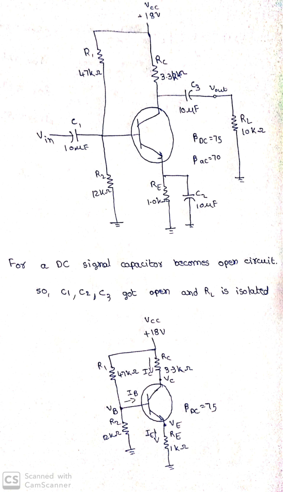
For a DC signal capacitor becomes open circuit.
The transistor in the given circuit is NPN transistor.
For an NPN transistor Vbe=0.7v
Collect current = Beta × Base current
Emitter current= Base current+ Collector current
ie=ib+ic


Add Answer to:
Question No. 4 |Marks 10, CLO 41 Determine the following DC values for the amplifier in...
b) An amplifier has values of V = 24mV and Vout gain of the circuit 2V....
 b) An amplifier has values of V = 24mV and Vout gain of the circuit 2V. Calculate the dB voltage (2 marks) c) For the circuit shown in Figure 11, calculate the lower critical frequency due to the output RC circuit. Vec +15 V R 3.9 LO C V. R. 0.33 uF 2N3904 600 n 0.1 F 5.6 k REI 33 0 R 22 k 50 mVpp 1.5 k 100 F (5 marks) Figure 11 12. a) Name the type...
5. Determine the following parameters for the amplifier of figure 4. Assume B= 150 and VA-...
 5. Determine the following parameters for the amplifier of figure 4. Assume B= 150 and VA- 120V. a. ICQ and VCEO b. Rin ܟܘ ܝܟ ܢܽܘ ܝܺ C. Ro d. Av(NL) Av(WL) 16 V R; 75 kq Rc 34.3 k2 10 uf 10 F E 2N2222A Rs 2ks R: 315ko Run $ 3302 RL 34740 v. 100 mV Re $1.6k9100 uF
QUESTION4 Total 24 Marks] For the amplifier circuit shown in Figure 4, assume the input signal...
 QUESTION4 Total 24 Marks] For the amplifier circuit shown in Figure 4, assume the input signal V has zero DC component. Assume both transistors have p-100. (a) State the type of feedback topology used in the amplifier circuit and which type of 12 marks] amplifier is shown in the figure. (b Determine the DC voltages at all nodes of transistors Q1 and Q2. and the DC currents 18 marks] at the emitters of transistors Q1 and Q2 (c) Use the...
3. In Figure 3, the DC operating point for BJT Q, is Ici = 170 uA...
 3. In Figure 3, the DC operating point for BJT Q, is Ici = 170 uA and VCE = 4 V, and the DC operating point for BJT 02 is Ic2 = 240 A and VCE2 = 3 V. Both Q1 and Q2 have B = 100, VA-75 V at the room temperature. Assume that all the capacitors have infinite values, and all the resistors have the values as indicated in Figure 3. (a) (b) Determine the voltage gain 4....
18. Determine the following ac values for the amplifier in Figure below. (c) A, (e) Ap...
 18. Determine the following ac values for the amplifier in Figure below. (c) A, (e) Ap (a) Rin (b) Rin(tot) (d) A¡ Vcc +18 V Rc 3.3 kn C2 ER 47 kN o Vout 104F βρC 75 10 mV B = 70 10μF C3 100 µF RE R, 12 k2 1.0 kN
Question 1 (10 marks) Figure 10 Rc2 shunt-shunt28R feedback amplifier circuit The resistors values and the transistors parameters are also indicated in Figure 1 1,-0.3mA 285m Hint: in DC analysis...
 Question 1 (10 marks) Figure 10 Rc2 shunt-shunt28R feedback amplifier circuit The resistors values and the transistors parameters are also indicated in Figure 1 1,-0.3mA 285m Hint: in DC analysis; 1) For R,-104, determine the small-signal closed-loop current-gain'. 2) Determine the small-signal open-loop current-gain 3) From the results of 2) and 3), determine the loop-gain T: Hint: If you did not solve 2), assume If you did not solve 3), assume600
Question 1 (10 marks) Figure 10 Rc2 shunt-shunt28R feedback...
Question 1 (10 marks) Figure 10 Rc2 shunt-shunt28R feedback amplifier circuit The resistors values and the transistors parameters are also indicated in Figure 1 1,-0.3mA 285m Hint: in DC analysis; 1) For R,-104, determine the small-signal closed-loop current-gain'. 2) Determine the small-signal open-loop current-gain 3) From the results of 2) and 3), determine the loop-gain T: Hint: If you did not solve 2), assume If you did not solve 3), assume600
Question 1 (10 marks) Figure 10 Rc2 shunt-shunt28R feedback...
11. (5 marks total) A common-emitter amplifier has values of R = 68 k 2, R2...
 11. (5 marks total) A common-emitter amplifier has values of R = 68 k 2, R2 = 56 k 2, Rinbase) = 2.1 k 2. The source voltage V, = 35 mV and the source resistance R = 450 22. Determine: Base R, w Base W- Rinas) Riiton = (a) (b) a) (3 marks) the total input resistance Rin(tot) = b) (2 marks) the voltage at the base (V=Vin) V = 9 12. (5 marks total) For the common-emitter amplifier...
pls answer all and asap.tqvm. (a) () What is the significant used of multistage amplifier compared...
 pls
answer all and asap.tqvm.
(a) () What is the significant used of multistage amplifier compared to single stage amplifier? (2 marks) (ii) In terms of circuit connection, how to differentiate between direct and capacitively coupled amplifier circuit? (1 mark) (ii) Give a reason why the capacitively coupled amplifier circuit is not suitable for amplifying DC voltage? (2 marks) (b) The multistage amplifier circuit of Figure Q.3 have the following parameters: Q1, Q2: B = 200, VBE = 0.7 V,....
pls
answer all and asap.tqvm.
(a) () What is the significant used of multistage amplifier compared to single stage amplifier? (2 marks) (ii) In terms of circuit connection, how to differentiate between direct and capacitively coupled amplifier circuit? (1 mark) (ii) Give a reason why the capacitively coupled amplifier circuit is not suitable for amplifying DC voltage? (2 marks) (b) The multistage amplifier circuit of Figure Q.3 have the following parameters: Q1, Q2: B = 200, VBE = 0.7 V,....
1. Figure 1 shows a CE power amplifier in which the collector resistor serves also as...
 1. Figure 1 shows a CE power amplifier in which the collector resistor serves also as the load resistor. Assume Bpc Bac 100 a. Determine the dc Q-point (lco and VCEQ). b. Determine the voltage gain and the power gain c. The power dissipated in the transistor with no load. d. The total power from the power supply with no load e. The signal power in the load with a 500 mV input. f. What changes would be necessary to...
a) Determine the DC bias voltage Vce and the current Ic for the voltage divider configuration...
 a) Determine the DC bias voltage Vce and the current Ic for the voltage divider configuration in Fig. 11. [4.0 marks] +22 V 10 k92 39k92 10 F HE 10 uF ti VE B = 100 3.9 k2 50uF Figure 11 b) Provide the construction diagram of n-channel JFET ii. n-channel depletion type MOSFET iii. n-channel Enhancement type MOSFET i. [3.0 marks) c) Describe the operation of an NPN transistor in the common-emitter (CE) configuration with aid of input and...
 b) An amplifier has values of V = 24mV and Vout gain of the circuit 2V. Calculate the dB voltage (2 marks) c) For the circuit shown in Figure 11, calculate the lower critical frequency due to the output RC circuit. Vec +15 V R 3.9 LO C V. R. 0.33 uF 2N3904 600 n 0.1 F 5.6 k REI 33 0 R 22 k 50 mVpp 1.5 k 100 F (5 marks) Figure 11 12. a) Name the type...
 5. Determine the following parameters for the amplifier of figure 4. Assume B= 150 and VA- 120V. a. ICQ and VCEO b. Rin ܟܘ ܝܟ ܢܽܘ ܝܺ C. Ro d. Av(NL) Av(WL) 16 V R; 75 kq Rc 34.3 k2 10 uf 10 F E 2N2222A Rs 2ks R: 315ko Run $ 3302 RL 34740 v. 100 mV Re $1.6k9100 uF
 QUESTION4 Total 24 Marks] For the amplifier circuit shown in Figure 4, assume the input signal V has zero DC component. Assume both transistors have p-100. (a) State the type of feedback topology used in the amplifier circuit and which type of 12 marks] amplifier is shown in the figure. (b Determine the DC voltages at all nodes of transistors Q1 and Q2. and the DC currents 18 marks] at the emitters of transistors Q1 and Q2 (c) Use the...
 3. In Figure 3, the DC operating point for BJT Q, is Ici = 170 uA and VCE = 4 V, and the DC operating point for BJT 02 is Ic2 = 240 A and VCE2 = 3 V. Both Q1 and Q2 have B = 100, VA-75 V at the room temperature. Assume that all the capacitors have infinite values, and all the resistors have the values as indicated in Figure 3. (a) (b) Determine the voltage gain 4....
 18. Determine the following ac values for the amplifier in Figure below. (c) A, (e) Ap (a) Rin (b) Rin(tot) (d) A¡ Vcc +18 V Rc 3.3 kn C2 ER 47 kN o Vout 104F βρC 75 10 mV B = 70 10μF C3 100 µF RE R, 12 k2 1.0 kN
 Question 1 (10 marks) Figure 10 Rc2 shunt-shunt28R feedback amplifier circuit The resistors values and the transistors parameters are also indicated in Figure 1 1,-0.3mA 285m Hint: in DC analysis; 1) For R,-104, determine the small-signal closed-loop current-gain'. 2) Determine the small-signal open-loop current-gain 3) From the results of 2) and 3), determine the loop-gain T: Hint: If you did not solve 2), assume If you did not solve 3), assume600
Question 1 (10 marks) Figure 10 Rc2 shunt-shunt28R feedback...
Question 1 (10 marks) Figure 10 Rc2 shunt-shunt28R feedback amplifier circuit The resistors values and the transistors parameters are also indicated in Figure 1 1,-0.3mA 285m Hint: in DC analysis; 1) For R,-104, determine the small-signal closed-loop current-gain'. 2) Determine the small-signal open-loop current-gain 3) From the results of 2) and 3), determine the loop-gain T: Hint: If you did not solve 2), assume If you did not solve 3), assume600
Question 1 (10 marks) Figure 10 Rc2 shunt-shunt28R feedback...
 11. (5 marks total) A common-emitter amplifier has values of R = 68 k 2, R2 = 56 k 2, Rinbase) = 2.1 k 2. The source voltage V, = 35 mV and the source resistance R = 450 22. Determine: Base R, w Base W- Rinas) Riiton = (a) (b) a) (3 marks) the total input resistance Rin(tot) = b) (2 marks) the voltage at the base (V=Vin) V = 9 12. (5 marks total) For the common-emitter amplifier...
 pls
answer all and asap.tqvm.
(a) () What is the significant used of multistage amplifier compared to single stage amplifier? (2 marks) (ii) In terms of circuit connection, how to differentiate between direct and capacitively coupled amplifier circuit? (1 mark) (ii) Give a reason why the capacitively coupled amplifier circuit is not suitable for amplifying DC voltage? (2 marks) (b) The multistage amplifier circuit of Figure Q.3 have the following parameters: Q1, Q2: B = 200, VBE = 0.7 V,....
pls
answer all and asap.tqvm.
(a) () What is the significant used of multistage amplifier compared to single stage amplifier? (2 marks) (ii) In terms of circuit connection, how to differentiate between direct and capacitively coupled amplifier circuit? (1 mark) (ii) Give a reason why the capacitively coupled amplifier circuit is not suitable for amplifying DC voltage? (2 marks) (b) The multistage amplifier circuit of Figure Q.3 have the following parameters: Q1, Q2: B = 200, VBE = 0.7 V,....
 1. Figure 1 shows a CE power amplifier in which the collector resistor serves also as the load resistor. Assume Bpc Bac 100 a. Determine the dc Q-point (lco and VCEQ). b. Determine the voltage gain and the power gain c. The power dissipated in the transistor with no load. d. The total power from the power supply with no load e. The signal power in the load with a 500 mV input. f. What changes would be necessary to...
 a) Determine the DC bias voltage Vce and the current Ic for the voltage divider configuration in Fig. 11. [4.0 marks] +22 V 10 k92 39k92 10 F HE 10 uF ti VE B = 100 3.9 k2 50uF Figure 11 b) Provide the construction diagram of n-channel JFET ii. n-channel depletion type MOSFET iii. n-channel Enhancement type MOSFET i. [3.0 marks) c) Describe the operation of an NPN transistor in the common-emitter (CE) configuration with aid of input and...
Most questions answered within 3 hours.
-
Where is the error in this code sequence?
String s1 = "Hello";
String s2 = "ello";...
asked 10 months ago -
Financial data for Joel de Paris, Inc., for last year
follow:
Joel de Paris, Inc.
Balance...
asked 10 months ago -
Consider this reaction:
Al2(SO4)3 (aq)+ BaCl3
(aq) Al2Cl6 (aq)- +
3BaSO4(s) . What is the...
asked 10 months ago -
Suppose that Savneet is considering increasing her
recent random sample from 20 car rentals to 40...
asked 10 months ago -
Trucks arrive at an unloading terminal at an average rate of 120
per hour.
Trucks arrive...
asked 10 months ago -
Why are methanol and ethanol completely soluble in water while
octanol is not very little soluble....
asked 10 months ago -
A facilities manager at a university reads in a research report
that the mean amount of...
asked 10 months ago -
When the CuSO4 is rehydrated by adding water to the anhydrous
compound, is this an endothermic...
asked 10 months ago -
A ray of sunlight is passing from diamond into crown glass; the
angle of incidence is...
asked 10 months ago -
A block of mass 0.249 kg is placed on top of a light, vertical
spring of...
asked 10 months ago -
how do the kidneys compensate in the presences of acidosis
a) trigger hyperventilate
b) reserve acid...
asked 10 months ago -
Question 501 pts
The rental rate of capital to the firm increases. Which of the
following...
asked 10 months ago