1) LT SPICE, select a diode, get characteristic chart 2) make Nand and Nor with transistor...
Homework Answers
1 TO DRAW THE CHARACTERISTICS OF THE DIODE.
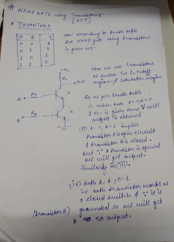
 2 TO MAKE NAND and NOR GATE
WITH TRANSISTOR.
2 TO MAKE NAND and NOR GATE
WITH TRANSISTOR.

3 CHARACTERISTICS OF JFET.

Add Answer to:
1)
LT SPICE, select a diode, get characteristic chart 2) make Nand and
Nor with transistor...
Please help with the LT SPICE for this nmos transistor analysis problem. I figured out the calcul...
 please help with the LT SPICE for this nmos transistor analysis
problem. I figured out the calculations, I just need help verifying
them with LT SPICE. thank you!
Analyze the following MOSFET circuit for dc bias. Solve for ID, VGs and VDs Use RD-5 kQ, Rs-5 kQ, RG,-1 ΜΩ and RG2-1 MS2. Use a power supply with VDD-| 2 V and K.-I mA/V2 and Vin-1 V. RG RD RG2 Rs Verify the analysis of the circuit of Prob. 5 by...
please help with the LT SPICE for this nmos transistor analysis
problem. I figured out the calculations, I just need help verifying
them with LT SPICE. thank you!
Analyze the following MOSFET circuit for dc bias. Solve for ID, VGs and VDs Use RD-5 kQ, Rs-5 kQ, RG,-1 ΜΩ and RG2-1 MS2. Use a power supply with VDD-| 2 V and K.-I mA/V2 and Vin-1 V. RG RD RG2 Rs Verify the analysis of the circuit of Prob. 5 by...
Question 1: An ideal diode turns on for positive anode-cathode voltages. But the characteristic of diode...
 Question 1: An ideal diode turns on for positive anode-cathode voltages. But the characteristic of diode does not appear to show any ID values when voltage across the diode is greater than zero (VD > 0). How do you explain this plot? ---Reverse bias Forward bias --- Question 2: Plot (I-V) characteristic if we place a 10 12 resistor in series with the diode? Question 3: Plot (I-V) characteristic if we place a lV voltage source in series with the...
1. What logic gates are known as universal gates? (1 point) a) nand, nor b) and,...
 1. What logic gates are known as universal gates? (1 point) a) nand, nor b) and, or, not c) nand, nor, xor, xnor d) None of the above 2. Write the half adder truth table. (4 points) 3. Fill in the blank. (1 point) A2 to 1 mux has input lines. 4. True or False? (1 point) A Boolean algebraic sum of products expression is the complement of the product of sums expression. 5. What is the minimum POS expression...
[10] Question 2: Fig. 1 shows a logic function, implemented by NOR gates. Please answer the...
 [10] Question 2: Fig. 1 shows a logic function, implemented by NOR gates. Please answer the following X1 X2 De X3 Fig. 1: Logic function. questions: 1) What is the logic function of the output in the form of product-of-sum? 2) Based on the derived logic function, please sketch transistor level compound gates. Assume both truth and complementary inputs are provided. 3) In many cases, more than 3 inputs may be required to carry out a logic function, e.g. 3-input...
Page 4 3. (a) Explain howa p-njunction can be used to make a diode laser. 4...
 Page 4 3. (a) Explain howa p-njunction can be used to make a diode laser. 4 marks (b) Sketch the ideal diode laser characteristic, indicating the spontaneous emission and stimulated emission regions and the threshold current. 2 marks State the threshold condition for laser action to occur in a laser diode of length L, absorption coefficient a, and gain coefficient y. The reflectivities of the cleaved planes of the laser diode are ri and F2 respectively. 1 marks Calculate the...
Page 4 3. (a) Explain howa p-njunction can be used to make a diode laser. 4...
 Page 4 3. (a) Explain howa p-njunction can be used to make a diode laser. 4 marks (b) Sketch the ideal diode laser characteristic, indicating the spontaneous emission and stimulated emission regions and the threshold current. 2 marks State the threshold condition for laser action to occur in a laser diode of length L, absorption coefficient a, and gain coefficient y. The reflectivities of the cleaved planes of the laser diode are ry and F2 respectively. 1 marks Calculate the...
1. Determine 2 ways to implement an inverter with a 2-input NAND gate. 2. Implement a...
1. Determine 2 ways to implement an inverter with a 2-input NAND gate. 2. Implement a 3-input NAND gate function using 2-input NAND gates only, draw schematics. 3. Implement a 2-input OR function using 2-input NAND gates only, draw schematics. 4. (A) Implement the function using one 2-input OR gate, one 2- input AND gate and one 2-input NAND gate. (B) Implement the same function with only NAND gates. (C) Make up the truth table for the function. What is...
1. at what voltage the current density in a p-n diode reaches a magnitude of 10 A/cm^2 ? the diode is made by doping with boron are phosphorous with concentrations of 10^18 and 10^19 cm^-3, respec...
 1. at what voltage the current density in a p-n diode
reaches a magnitude of 10 A/cm^2 ? the diode is made by doping with
boron are phosphorous with concentrations of 10^18 and 10^19 cm^-3,
respectively.
3. A MOSFET is made on silicon substrate doped with boron with a concentration of 10" cm. Width and length of channel are 100 and O.1 micron respectively. Thickness of the oxide insulator under the gate is 10 nm. Find transconductance of this transistor...
1. at what voltage the current density in a p-n diode
reaches a magnitude of 10 A/cm^2 ? the diode is made by doping with
boron are phosphorous with concentrations of 10^18 and 10^19 cm^-3,
respectively.
3. A MOSFET is made on silicon substrate doped with boron with a concentration of 10" cm. Width and length of channel are 100 and O.1 micron respectively. Thickness of the oxide insulator under the gate is 10 nm. Find transconductance of this transistor...
Question 1: Select the single correct answer [2 marks each] Which of the following statements is ...
 CMOS VLSI DESIGN, Please attempt all the
objective type questions.CMOS
Question 1: Select the single correct answer [2 marks each] Which of the following statements is true for a MOSFET switch (input is gate node)? A) nMOS is off with logic I' at input B) nMOS is on with logic '1' at input C) pMOS is on with logic '1' at input' D) pMOS is off with logic '0' at input Which of the following CMOS logic circuits will contain...
CMOS VLSI DESIGN, Please attempt all the
objective type questions.CMOS
Question 1: Select the single correct answer [2 marks each] Which of the following statements is true for a MOSFET switch (input is gate node)? A) nMOS is off with logic I' at input B) nMOS is on with logic '1' at input C) pMOS is on with logic '1' at input' D) pMOS is off with logic '0' at input Which of the following CMOS logic circuits will contain...
Laboratory 2: Transistor circuit characteristics A. Objectives: 1. To study the basic characteris...
 Laboratory 2: Transistor circuit characteristics A. Objectives: 1. To study the basic characteristics of a transistor circuit. 2. To study the bias circuit of a transistor circuit. B. Apparatus: 1. DC Power supply 2. Experimental boards and corresponding components 3. Electronic calculator (prepared by students) 4. Digital camera (prepared by students for photo taking of the experimental results) 5. Laptop computer with the software PicoScope 6 and Microsoft Word installed. 6. PicoScope PC Oscilloscope and its accessories. 7. Digital multi-meter....
 please help with the LT SPICE for this nmos transistor analysis
problem. I figured out the calculations, I just need help verifying
them with LT SPICE. thank you!
Analyze the following MOSFET circuit for dc bias. Solve for ID, VGs and VDs Use RD-5 kQ, Rs-5 kQ, RG,-1 ΜΩ and RG2-1 MS2. Use a power supply with VDD-| 2 V and K.-I mA/V2 and Vin-1 V. RG RD RG2 Rs Verify the analysis of the circuit of Prob. 5 by...
please help with the LT SPICE for this nmos transistor analysis
problem. I figured out the calculations, I just need help verifying
them with LT SPICE. thank you!
Analyze the following MOSFET circuit for dc bias. Solve for ID, VGs and VDs Use RD-5 kQ, Rs-5 kQ, RG,-1 ΜΩ and RG2-1 MS2. Use a power supply with VDD-| 2 V and K.-I mA/V2 and Vin-1 V. RG RD RG2 Rs Verify the analysis of the circuit of Prob. 5 by...
 Question 1: An ideal diode turns on for positive anode-cathode voltages. But the characteristic of diode does not appear to show any ID values when voltage across the diode is greater than zero (VD > 0). How do you explain this plot? ---Reverse bias Forward bias --- Question 2: Plot (I-V) characteristic if we place a 10 12 resistor in series with the diode? Question 3: Plot (I-V) characteristic if we place a lV voltage source in series with the...
 1. What logic gates are known as universal gates? (1 point) a) nand, nor b) and, or, not c) nand, nor, xor, xnor d) None of the above 2. Write the half adder truth table. (4 points) 3. Fill in the blank. (1 point) A2 to 1 mux has input lines. 4. True or False? (1 point) A Boolean algebraic sum of products expression is the complement of the product of sums expression. 5. What is the minimum POS expression...
 [10] Question 2: Fig. 1 shows a logic function, implemented by NOR gates. Please answer the following X1 X2 De X3 Fig. 1: Logic function. questions: 1) What is the logic function of the output in the form of product-of-sum? 2) Based on the derived logic function, please sketch transistor level compound gates. Assume both truth and complementary inputs are provided. 3) In many cases, more than 3 inputs may be required to carry out a logic function, e.g. 3-input...
 Page 4 3. (a) Explain howa p-njunction can be used to make a diode laser. 4 marks (b) Sketch the ideal diode laser characteristic, indicating the spontaneous emission and stimulated emission regions and the threshold current. 2 marks State the threshold condition for laser action to occur in a laser diode of length L, absorption coefficient a, and gain coefficient y. The reflectivities of the cleaved planes of the laser diode are ri and F2 respectively. 1 marks Calculate the...
 Page 4 3. (a) Explain howa p-njunction can be used to make a diode laser. 4 marks (b) Sketch the ideal diode laser characteristic, indicating the spontaneous emission and stimulated emission regions and the threshold current. 2 marks State the threshold condition for laser action to occur in a laser diode of length L, absorption coefficient a, and gain coefficient y. The reflectivities of the cleaved planes of the laser diode are ry and F2 respectively. 1 marks Calculate the...
 1. at what voltage the current density in a p-n diode
reaches a magnitude of 10 A/cm^2 ? the diode is made by doping with
boron are phosphorous with concentrations of 10^18 and 10^19 cm^-3,
respectively.
3. A MOSFET is made on silicon substrate doped with boron with a concentration of 10" cm. Width and length of channel are 100 and O.1 micron respectively. Thickness of the oxide insulator under the gate is 10 nm. Find transconductance of this transistor...
1. at what voltage the current density in a p-n diode
reaches a magnitude of 10 A/cm^2 ? the diode is made by doping with
boron are phosphorous with concentrations of 10^18 and 10^19 cm^-3,
respectively.
3. A MOSFET is made on silicon substrate doped with boron with a concentration of 10" cm. Width and length of channel are 100 and O.1 micron respectively. Thickness of the oxide insulator under the gate is 10 nm. Find transconductance of this transistor...
 CMOS VLSI DESIGN, Please attempt all the
objective type questions.CMOS
Question 1: Select the single correct answer [2 marks each] Which of the following statements is true for a MOSFET switch (input is gate node)? A) nMOS is off with logic I' at input B) nMOS is on with logic '1' at input C) pMOS is on with logic '1' at input' D) pMOS is off with logic '0' at input Which of the following CMOS logic circuits will contain...
CMOS VLSI DESIGN, Please attempt all the
objective type questions.CMOS
Question 1: Select the single correct answer [2 marks each] Which of the following statements is true for a MOSFET switch (input is gate node)? A) nMOS is off with logic I' at input B) nMOS is on with logic '1' at input C) pMOS is on with logic '1' at input' D) pMOS is off with logic '0' at input Which of the following CMOS logic circuits will contain...
 Laboratory 2: Transistor circuit characteristics A. Objectives: 1. To study the basic characteristics of a transistor circuit. 2. To study the bias circuit of a transistor circuit. B. Apparatus: 1. DC Power supply 2. Experimental boards and corresponding components 3. Electronic calculator (prepared by students) 4. Digital camera (prepared by students for photo taking of the experimental results) 5. Laptop computer with the software PicoScope 6 and Microsoft Word installed. 6. PicoScope PC Oscilloscope and its accessories. 7. Digital multi-meter....
Most questions answered within 3 hours.
-
Where is the error in this code sequence?
String s1 = "Hello";
String s2 = "ello";...
asked 10 months ago -
Financial data for Joel de Paris, Inc., for last year
follow:
Joel de Paris, Inc.
Balance...
asked 10 months ago -
Consider this reaction:
Al2(SO4)3 (aq)+ BaCl3
(aq) Al2Cl6 (aq)- +
3BaSO4(s) . What is the...
asked 10 months ago -
Suppose that Savneet is considering increasing her
recent random sample from 20 car rentals to 40...
asked 10 months ago -
Trucks arrive at an unloading terminal at an average rate of 120
per hour.
Trucks arrive...
asked 10 months ago -
Why are methanol and ethanol completely soluble in water while
octanol is not very little soluble....
asked 10 months ago -
A facilities manager at a university reads in a research report
that the mean amount of...
asked 10 months ago -
When the CuSO4 is rehydrated by adding water to the anhydrous
compound, is this an endothermic...
asked 10 months ago -
A ray of sunlight is passing from diamond into crown glass; the
angle of incidence is...
asked 10 months ago -
A block of mass 0.249 kg is placed on top of a light, vertical
spring of...
asked 10 months ago -
how do the kidneys compensate in the presences of acidosis
a) trigger hyperventilate
b) reserve acid...
asked 10 months ago -
Question 501 pts
The rental rate of capital to the firm increases. Which of the
following...
asked 10 months ago