
Homework Answers

Add Answer to:
Q2 (24%) A Si PN junction is operating at 300K. The device parameters are as follows:...
A silicon PN junction diode is constructed using N-type silicon in which the Fermi level is...
 A silicon PN junction diode is constructed using N-type silicon in which the Fermi level is 100 meV below the conduction band edge and P-type silicon in which the Fermi level is 120 meV above the valence band edge a) What are the majority and minority carrier concentrations on each side of the junction under thermal equilibrium? b) What is the value of the built-in voltage? c) Determine the width of the depletion region on both sides of the junction...
Assume a p-n step junction in silicon wi concentration of 2x10¹⁶,c? and the n-type material doped...
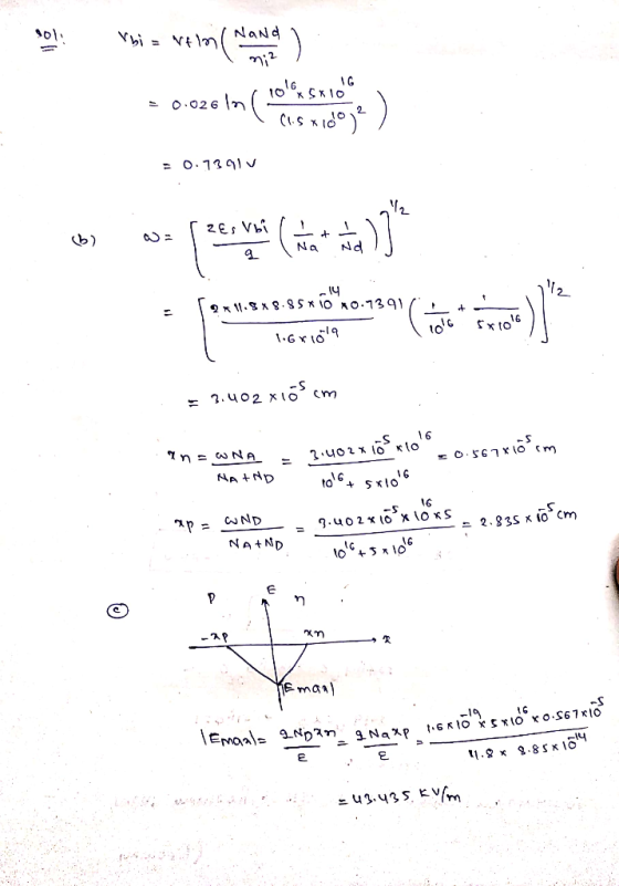
 Assume a p-n step junction in silicon wi concentration of 2x10¹⁶,c? and the n-type material doped at 3X10-s,cm3 The intrinsic carrier density is 1.25X101°/cm and all dopants are fully ionized Assume that the effective density of states for silicon is 3.3x10 cm3 for the conduction band and 1.75x101 cm for the valence band. Assume that the temperature is 300K and silicon relative permittivity of 11.7 a. Compute the hole concentration on the n-side and electron concentration th the p-type material...
The parameters of a pn junction diode at 300K are listed in the following table, the...
 The parameters of a pn junction diode at 300K are listed in the following table, the cross section area of the junction is 105 cm2 n region N10" cm Hu = 850 cm?/V-s p region t,e = 10-6 s ,1" 1250 cm2/V-s 11,-420 cm2/V-s 320 cm/V-s (a) Sketch a band diagram at equilibrium (b) Find the reserve saturation current (c) Find the ideal diode current with forward bias voltage at 0.5 V and 0.7 V, respectively. (d) Find the current...
A pn iunction diode has the following parameters, Na-2x10^17 Dp 10.36 Tp - 5x10-'s Area is...
 A pn iunction diode has the following parameters, Na-2x10^17 Dp 10.36 Tp - 5x10-'s Area is 1mm 2 Nc-1x10 16 Dn-18.13 Tn-5x10-s Length of diode is 100 mm At equilibrium, what is the width of the depletion region, the built in potential, the electric field across the depletion region and the capacitance of the depletion region a. b. Can you tell from the doping levels which region the depletion regioin c. Find the Fermi level in both regions and the...
Problem 4: Narrow-Base Diode Consider an ideal pn* step-junction Si diode maintained at 300K with cross-sectional...
 Problem 4: Narrow-Base Diode Consider an ideal pn* step-junction Si diode maintained at 300K with cross-sectional area A = 104cm2. The doping concentration on the p-type side is Na= 1017 cm3 (uncompensated). (The n-type side is degenerately doped.) The electron recombination lifetime in the p-type region is tn = 10-6 s. The width of the quasi-neutral p-type region is 1 um, for VA=0 V. a Is this a narrow-base diode? Justify your answer. b) Calculate the diode saturation current Io....
Problem 1 (25 points) Consider a silicon pn junction with a cross section area of 1x105 cm, a forward bias Va 0.5V, and the following parameters at T- 300K: 16cm-3 15 3 -6 KT n: 1.5x100 cm", ε...
 Problem 1 (25 points) Consider a silicon pn junction with a cross section area of 1x105 cm, a forward bias Va 0.5V, and the following parameters at T- 300K: 16cm-3 15 3 -6 KT n: 1.5x100 cm", ε' = 1 1 .7x 8.854x 10-14 Flon;ー-0.025 V Assume the critical field to be equal to 3x10⁵ V/cm. a) (5 points) Compare the hole density at xn to the electron density at-Xp b) (5 points) Compare the hole current at xn to...
A silicon pn junction at T = 300 K has the following parameters: Na-5 1016 cm-?,...
 A silicon pn junction at T = 300 K has the following parameters: Na-5 1016 cm-?, N,-1 1016 cm-3, D.-25 cm3/s, D.-10 cm2/s, ?,0-5 x 10⁻⁷ s, and To 1 X 10⁻⁷ s. The cross-sectional area is A 10-3 cm2 and the forward- bias voltage is V,-0.625 V. Calculate the (a) minority electron diffusion cur- rent at the space charge edge, (b) minority hole diffusion current at the space charge edge, and (c) total current in the pn junction diode.
this is a problem of semiconductor device and fundamentals. Problem 4: pn Junction Current Distributions Consider a...
 this is a problem of semiconductor device and
fundamentals.
Problem 4: pn Junction Current Distributions Consider a Si pn step junction diode maintained at room temperature, with p-side and n-side dopant concentrations NA 1016 cm3 and Np-2x1016 cm3, respectively. (You may assume that each side is uncompensated.) The minority carrier recombination lifetimes are τ,-10-6 s and τ,-10-7 s on the p-side and n-side, respectively a) Calculate the minority carrier densities at the edges of the depletion region when the applied...
this is a problem of semiconductor device and
fundamentals.
Problem 4: pn Junction Current Distributions Consider a Si pn step junction diode maintained at room temperature, with p-side and n-side dopant concentrations NA 1016 cm3 and Np-2x1016 cm3, respectively. (You may assume that each side is uncompensated.) The minority carrier recombination lifetimes are τ,-10-6 s and τ,-10-7 s on the p-side and n-side, respectively a) Calculate the minority carrier densities at the edges of the depletion region when the applied...
Design an ideal abrupt silicon PN-junction at 300 K such that the donor impurity concentration in...
 XXX is 467
Design an ideal abrupt silicon PN-junction at 300 K such that the donor impurity concentration in the n-side N, = 5x1015 cm3 and the acceptor impurity concentration in the p-side N, = XXX × 1015/cm3 Assume that the diode area A-2x10⁻³ cm2 and 100cm work Note that the values obtained in the calculations may not be realistic as the Matric # varies greatly. The assignment is only to test your understanding, and must be handwritten Determine the...
XXX is 467
Design an ideal abrupt silicon PN-junction at 300 K such that the donor impurity concentration in the n-side N, = 5x1015 cm3 and the acceptor impurity concentration in the p-side N, = XXX × 1015/cm3 Assume that the diode area A-2x10⁻³ cm2 and 100cm work Note that the values obtained in the calculations may not be realistic as the Matric # varies greatly. The assignment is only to test your understanding, and must be handwritten Determine the...
Problem 3 (25 points) Consider a silicon pn junction at T - 300 K, NA- 1016 cm3, ND-5x1016 cm-3. The minority carrier lifetimes are τα , τ,-1 us. The junction is forward biased with Va-0.5V The minor...
 Problem 3 (25 points) Consider a silicon pn junction at T - 300 K, NA- 1016 cm3, ND-5x1016 cm-3. The minority carrier lifetimes are τα , τ,-1 us. The junction is forward biased with Va-0.5V The minority carrier diffusion coefficients are D 25 cm/s, Da- 10 cm2/s n,1.5x1010 cm3 kT 0.0267 Depletion region p-type n-type a) (5 points) Calculate the excess electron concentration as a function of x in the p-side (see the figure above) b) (10 points) Calculate the...
 A silicon PN junction diode is constructed using N-type silicon in which the Fermi level is 100 meV below the conduction band edge and P-type silicon in which the Fermi level is 120 meV above the valence band edge a) What are the majority and minority carrier concentrations on each side of the junction under thermal equilibrium? b) What is the value of the built-in voltage? c) Determine the width of the depletion region on both sides of the junction...
 Assume a p-n step junction in silicon wi concentration of 2x10¹⁶,c? and the n-type material doped at 3X10-s,cm3 The intrinsic carrier density is 1.25X101°/cm and all dopants are fully ionized Assume that the effective density of states for silicon is 3.3x10 cm3 for the conduction band and 1.75x101 cm for the valence band. Assume that the temperature is 300K and silicon relative permittivity of 11.7 a. Compute the hole concentration on the n-side and electron concentration th the p-type material...
 The parameters of a pn junction diode at 300K are listed in the following table, the cross section area of the junction is 105 cm2 n region N10" cm Hu = 850 cm?/V-s p region t,e = 10-6 s ,1" 1250 cm2/V-s 11,-420 cm2/V-s 320 cm/V-s (a) Sketch a band diagram at equilibrium (b) Find the reserve saturation current (c) Find the ideal diode current with forward bias voltage at 0.5 V and 0.7 V, respectively. (d) Find the current...
 A pn iunction diode has the following parameters, Na-2x10^17 Dp 10.36 Tp - 5x10-'s Area is 1mm 2 Nc-1x10 16 Dn-18.13 Tn-5x10-s Length of diode is 100 mm At equilibrium, what is the width of the depletion region, the built in potential, the electric field across the depletion region and the capacitance of the depletion region a. b. Can you tell from the doping levels which region the depletion regioin c. Find the Fermi level in both regions and the...
 Problem 4: Narrow-Base Diode Consider an ideal pn* step-junction Si diode maintained at 300K with cross-sectional area A = 104cm2. The doping concentration on the p-type side is Na= 1017 cm3 (uncompensated). (The n-type side is degenerately doped.) The electron recombination lifetime in the p-type region is tn = 10-6 s. The width of the quasi-neutral p-type region is 1 um, for VA=0 V. a Is this a narrow-base diode? Justify your answer. b) Calculate the diode saturation current Io....
 Problem 1 (25 points) Consider a silicon pn junction with a cross section area of 1x105 cm, a forward bias Va 0.5V, and the following parameters at T- 300K: 16cm-3 15 3 -6 KT n: 1.5x100 cm", ε' = 1 1 .7x 8.854x 10-14 Flon;ー-0.025 V Assume the critical field to be equal to 3x10⁵ V/cm. a) (5 points) Compare the hole density at xn to the electron density at-Xp b) (5 points) Compare the hole current at xn to...
 A silicon pn junction at T = 300 K has the following parameters: Na-5 1016 cm-?, N,-1 1016 cm-3, D.-25 cm3/s, D.-10 cm2/s, ?,0-5 x 10⁻⁷ s, and To 1 X 10⁻⁷ s. The cross-sectional area is A 10-3 cm2 and the forward- bias voltage is V,-0.625 V. Calculate the (a) minority electron diffusion cur- rent at the space charge edge, (b) minority hole diffusion current at the space charge edge, and (c) total current in the pn junction diode.
 this is a problem of semiconductor device and
fundamentals.
Problem 4: pn Junction Current Distributions Consider a Si pn step junction diode maintained at room temperature, with p-side and n-side dopant concentrations NA 1016 cm3 and Np-2x1016 cm3, respectively. (You may assume that each side is uncompensated.) The minority carrier recombination lifetimes are τ,-10-6 s and τ,-10-7 s on the p-side and n-side, respectively a) Calculate the minority carrier densities at the edges of the depletion region when the applied...
this is a problem of semiconductor device and
fundamentals.
Problem 4: pn Junction Current Distributions Consider a Si pn step junction diode maintained at room temperature, with p-side and n-side dopant concentrations NA 1016 cm3 and Np-2x1016 cm3, respectively. (You may assume that each side is uncompensated.) The minority carrier recombination lifetimes are τ,-10-6 s and τ,-10-7 s on the p-side and n-side, respectively a) Calculate the minority carrier densities at the edges of the depletion region when the applied...
 XXX is 467
Design an ideal abrupt silicon PN-junction at 300 K such that the donor impurity concentration in the n-side N, = 5x1015 cm3 and the acceptor impurity concentration in the p-side N, = XXX × 1015/cm3 Assume that the diode area A-2x10⁻³ cm2 and 100cm work Note that the values obtained in the calculations may not be realistic as the Matric # varies greatly. The assignment is only to test your understanding, and must be handwritten Determine the...
XXX is 467
Design an ideal abrupt silicon PN-junction at 300 K such that the donor impurity concentration in the n-side N, = 5x1015 cm3 and the acceptor impurity concentration in the p-side N, = XXX × 1015/cm3 Assume that the diode area A-2x10⁻³ cm2 and 100cm work Note that the values obtained in the calculations may not be realistic as the Matric # varies greatly. The assignment is only to test your understanding, and must be handwritten Determine the...
 Problem 3 (25 points) Consider a silicon pn junction at T - 300 K, NA- 1016 cm3, ND-5x1016 cm-3. The minority carrier lifetimes are τα , τ,-1 us. The junction is forward biased with Va-0.5V The minority carrier diffusion coefficients are D 25 cm/s, Da- 10 cm2/s n,1.5x1010 cm3 kT 0.0267 Depletion region p-type n-type a) (5 points) Calculate the excess electron concentration as a function of x in the p-side (see the figure above) b) (10 points) Calculate the...
Most questions answered within 3 hours.
-
Where is the error in this code sequence?
String s1 = "Hello";
String s2 = "ello";...
asked 10 months ago -
Financial data for Joel de Paris, Inc., for last year
follow:
Joel de Paris, Inc.
Balance...
asked 10 months ago -
Consider this reaction:
Al2(SO4)3 (aq)+ BaCl3
(aq) Al2Cl6 (aq)- +
3BaSO4(s) . What is the...
asked 10 months ago -
Suppose that Savneet is considering increasing her
recent random sample from 20 car rentals to 40...
asked 10 months ago -
Trucks arrive at an unloading terminal at an average rate of 120
per hour.
Trucks arrive...
asked 10 months ago -
Why are methanol and ethanol completely soluble in water while
octanol is not very little soluble....
asked 10 months ago -
A facilities manager at a university reads in a research report
that the mean amount of...
asked 10 months ago -
When the CuSO4 is rehydrated by adding water to the anhydrous
compound, is this an endothermic...
asked 10 months ago -
A ray of sunlight is passing from diamond into crown glass; the
angle of incidence is...
asked 10 months ago -
A block of mass 0.249 kg is placed on top of a light, vertical
spring of...
asked 10 months ago -
how do the kidneys compensate in the presences of acidosis
a) trigger hyperventilate
b) reserve acid...
asked 10 months ago -
Question 501 pts
The rental rate of capital to the firm increases. Which of the
following...
asked 10 months ago