

Please only use PSpice as stated in the directions. Any other software will not be accepted. Thanks
No multisim or LTSpice.
Homework Answers
Case:1
R2=330k;Vbb=10v
Ib= (Vbb-Vbe)/R2= (10-0.7)/330k = 28.28 micro A.


________________________________________________________________________________
Case:2
R2=147k;Vbb=10v
Ib= (Vbb-Vbe)/R2= (10-0.7)/147k =63.26 micro A.


Add Answer to:
Please only use PSpice as stated in the directions. Any other
software will not be accepted....
Electronics-common emmitter amplifier. Pls be try to be helpful Im trying to study here in this book example.. However im kinda lost and i cant follow the correct answers they got.. could someon...
 Electronics-common emmitter amplifier. Pls be try to be
helpful
Im trying to study here in this book example..
However im kinda lost and i cant follow the correct answers
they got.. could someone pls help me..
I just wanna learn this, i hope u can help me learn by showin
clear and corect solutions on how to properly got the
answer..
Also especially on finding the values on the laod line
analysis, im lost.
Pls help
Any helpful help would...
Electronics-common emmitter amplifier. Pls be try to be
helpful
Im trying to study here in this book example..
However im kinda lost and i cant follow the correct answers
they got.. could someone pls help me..
I just wanna learn this, i hope u can help me learn by showin
clear and corect solutions on how to properly got the
answer..
Also especially on finding the values on the laod line
analysis, im lost.
Pls help
Any helpful help would...
4. Lab VIII: Experiment VII The Bipolar Junction Transistor (BJT) Characteristics The bipolar junction transistor (BJT)...
 4. Lab VIII: Experiment VII The Bipolar Junction Transistor (BJT) Characteristics The bipolar junction transistor (BJT) is a three-terminal solid state device widely used as an amplifier (or switching) device. It consists of two n-type materials sandwiched by p-type material (npn) or two p-type and n-type. The terminals (sections) are known as emitter E, base B and collector C. Two currents and two voltages uniquely describe the behavior of the device. The third current/voltage can be determined through KCL/KVL. See...
Electronics1. It's a multiple choices question. use the formula sheet if needed (the last picture). Question...
 Electronics1. It's a multiple choices question. use the formula
sheet if needed (the last picture).
Question 3 CIRCUIT B1 (2.5 Marks) + VC Rc IRC < + RB IC IB V ce → IE FIG. 3: CIRCUIT B1 Statement: Sketching relevant output (V-Ic) characteristics decide on Q-point coordinates and DC load-line details: That is, determine DC operating conditions of the NPN-BJT/Si circuit of Fig.3 (denoting the type Circuit B1). Assume the following: Vcc= 20 volt; Rc = 2.5 k; RB...
Electronics1. It's a multiple choices question. use the formula
sheet if needed (the last picture).
Question 3 CIRCUIT B1 (2.5 Marks) + VC Rc IRC < + RB IC IB V ce → IE FIG. 3: CIRCUIT B1 Statement: Sketching relevant output (V-Ic) characteristics decide on Q-point coordinates and DC load-line details: That is, determine DC operating conditions of the NPN-BJT/Si circuit of Fig.3 (denoting the type Circuit B1). Assume the following: Vcc= 20 volt; Rc = 2.5 k; RB...
PLEASE SHOW ALL WORK AND TO FOLLOW DIRECTIONS. PLEASE USE PSPICE. STUDENT ID= 7220849 2. Using...
 PLEASE SHOW ALL WORK AND TO FOLLOW DIRECTIONS. PLEASE USE
PSPICE.
STUDENT ID= 7220849
2. Using a DC Sweep analysis to generate a table of values in the .OUT file: See Circuit 2 below: Let R1 through R6 equivalent to the digits 1 through 6 in your StudentID in k12 (use 10 k22 for a digit of 0). • For example, if your StudentID is 9870654 then R1 =9 kN, R2 =8 kN, R3 = 7kN, R4 = 10KN, R5...
PLEASE SHOW ALL WORK AND TO FOLLOW DIRECTIONS. PLEASE USE
PSPICE.
STUDENT ID= 7220849
2. Using a DC Sweep analysis to generate a table of values in the .OUT file: See Circuit 2 below: Let R1 through R6 equivalent to the digits 1 through 6 in your StudentID in k12 (use 10 k22 for a digit of 0). • For example, if your StudentID is 9870654 then R1 =9 kN, R2 =8 kN, R3 = 7kN, R4 = 10KN, R5...
Electronics1. It's a multiple choices question. use the formula sheet if needed (the last picture). Question...
 Electronics1. It's a multiple choices question. use the formula
sheet if needed (the last picture).
Question 4 CIRCUIT B2 (2.5 Marks) +Voc R ler Vic RS IB Vc V. RE FIG.4: CIRCUIT B2 Statement: Sketching relevant output (VIC) characteristics decide on Q-point coordinates and DC load-line details: That is, determine DC operating conditions of the NPN-BJT/Si circuit of Fig. 4 (denoting the type Circuit B2). Assume the following: Vor = 24 volt; Rc = 5.0 k; Re = 1000 ohm:...
Electronics1. It's a multiple choices question. use the formula
sheet if needed (the last picture).
Question 4 CIRCUIT B2 (2.5 Marks) +Voc R ler Vic RS IB Vc V. RE FIG.4: CIRCUIT B2 Statement: Sketching relevant output (VIC) characteristics decide on Q-point coordinates and DC load-line details: That is, determine DC operating conditions of the NPN-BJT/Si circuit of Fig. 4 (denoting the type Circuit B2). Assume the following: Vor = 24 volt; Rc = 5.0 k; Re = 1000 ohm:...
PLEASE SHOW ALL WORK AND TO FOLLOW DIRECTIONS. PLEASE USE PSPICE. STUDENT ID= 7220849 3. Using...
 PLEASE SHOW ALL WORK AND TO FOLLOW DIRECTIONS. PLEASE USE
PSPICE.
STUDENT ID= 7220849
3. Using a DC Sweep analysis to graph currents and voltages Let R1 through R4 equivalent to the digits 1 through 4 in your StudentID in k 2 (use 10 k12 for a digit of 0). • For example, if your StudentID is 9870654 then R1 =9 KS2, R2 =8 kN, R3 = 7k2 and R4 = 10k12 A. Analyze Circuit 3 by hand to determine...
PLEASE SHOW ALL WORK AND TO FOLLOW DIRECTIONS. PLEASE USE
PSPICE.
STUDENT ID= 7220849
3. Using a DC Sweep analysis to graph currents and voltages Let R1 through R4 equivalent to the digits 1 through 4 in your StudentID in k 2 (use 10 k12 for a digit of 0). • For example, if your StudentID is 9870654 then R1 =9 KS2, R2 =8 kN, R3 = 7k2 and R4 = 10k12 A. Analyze Circuit 3 by hand to determine...
PLEASE SHOW ALL WORK AND TO USE PSPICE AND FOLLOW ALL DIRECTIONS. STUDENT ID=378564 Assignment: 1....
 PLEASE SHOW ALL WORK AND TO USE PSPICE AND FOLLOW ALL
DIRECTIONS.
STUDENT ID=378564
Assignment: 1. For the Circuit 1 shown below: A. Analyze the circuit by hand as described in the textbook. B. Analyze the circuit using PSPICE as follows: Use a Bias Point analysis to find the quantities found in part A above. Be sure to add text to the schematic as indicated in the Sample Report. Adjust the placement of each value on the schematic so that...
PLEASE SHOW ALL WORK AND TO USE PSPICE AND FOLLOW ALL
DIRECTIONS.
STUDENT ID=378564
Assignment: 1. For the Circuit 1 shown below: A. Analyze the circuit by hand as described in the textbook. B. Analyze the circuit using PSPICE as follows: Use a Bias Point analysis to find the quantities found in part A above. Be sure to add text to the schematic as indicated in the Sample Report. Adjust the placement of each value on the schematic so that...
Could someone please help me on how I should be configuring the circuit in Figure 4(a)...
 Could someone please help me on how I should be configuring the
circuit in Figure 4(a) in Multisim? Basically not understanding
question #1 in the Procedure. Cannot keep Vrb the same value while
adjusting Vcc. Then when trying to adjust Vbb to hold Vrb, Ib
changes.
Any help is appreciated!
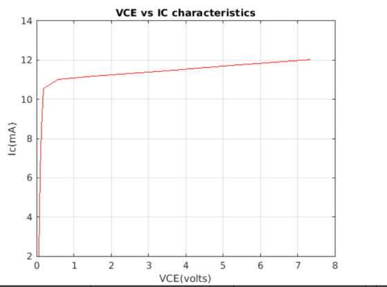
Discrete Devices Section LAB 4 BJT CHARACTERISTICS AND BIASING Objective: The objective of this laboratory is to examine the operation of a bipolar junction transistor and plot its output characteristics...
Could someone please help me on how I should be configuring the
circuit in Figure 4(a) in Multisim? Basically not understanding
question #1 in the Procedure. Cannot keep Vrb the same value while
adjusting Vcc. Then when trying to adjust Vbb to hold Vrb, Ib
changes.
Any help is appreciated!
Discrete Devices Section LAB 4 BJT CHARACTERISTICS AND BIASING Objective: The objective of this laboratory is to examine the operation of a bipolar junction transistor and plot its output characteristics...
 Electronics-common emmitter amplifier. Pls be try to be
helpful
Im trying to study here in this book example..
However im kinda lost and i cant follow the correct answers
they got.. could someone pls help me..
I just wanna learn this, i hope u can help me learn by showin
clear and corect solutions on how to properly got the
answer..
Also especially on finding the values on the laod line
analysis, im lost.
Pls help
Any helpful help would...
Electronics-common emmitter amplifier. Pls be try to be
helpful
Im trying to study here in this book example..
However im kinda lost and i cant follow the correct answers
they got.. could someone pls help me..
I just wanna learn this, i hope u can help me learn by showin
clear and corect solutions on how to properly got the
answer..
Also especially on finding the values on the laod line
analysis, im lost.
Pls help
Any helpful help would...
 4. Lab VIII: Experiment VII The Bipolar Junction Transistor (BJT) Characteristics The bipolar junction transistor (BJT) is a three-terminal solid state device widely used as an amplifier (or switching) device. It consists of two n-type materials sandwiched by p-type material (npn) or two p-type and n-type. The terminals (sections) are known as emitter E, base B and collector C. Two currents and two voltages uniquely describe the behavior of the device. The third current/voltage can be determined through KCL/KVL. See...
 Electronics1. It's a multiple choices question. use the formula
sheet if needed (the last picture).
Question 3 CIRCUIT B1 (2.5 Marks) + VC Rc IRC < + RB IC IB V ce → IE FIG. 3: CIRCUIT B1 Statement: Sketching relevant output (V-Ic) characteristics decide on Q-point coordinates and DC load-line details: That is, determine DC operating conditions of the NPN-BJT/Si circuit of Fig.3 (denoting the type Circuit B1). Assume the following: Vcc= 20 volt; Rc = 2.5 k; RB...
Electronics1. It's a multiple choices question. use the formula
sheet if needed (the last picture).
Question 3 CIRCUIT B1 (2.5 Marks) + VC Rc IRC < + RB IC IB V ce → IE FIG. 3: CIRCUIT B1 Statement: Sketching relevant output (V-Ic) characteristics decide on Q-point coordinates and DC load-line details: That is, determine DC operating conditions of the NPN-BJT/Si circuit of Fig.3 (denoting the type Circuit B1). Assume the following: Vcc= 20 volt; Rc = 2.5 k; RB...
 PLEASE SHOW ALL WORK AND TO FOLLOW DIRECTIONS. PLEASE USE
PSPICE.
STUDENT ID= 7220849
2. Using a DC Sweep analysis to generate a table of values in the .OUT file: See Circuit 2 below: Let R1 through R6 equivalent to the digits 1 through 6 in your StudentID in k12 (use 10 k22 for a digit of 0). • For example, if your StudentID is 9870654 then R1 =9 kN, R2 =8 kN, R3 = 7kN, R4 = 10KN, R5...
PLEASE SHOW ALL WORK AND TO FOLLOW DIRECTIONS. PLEASE USE
PSPICE.
STUDENT ID= 7220849
2. Using a DC Sweep analysis to generate a table of values in the .OUT file: See Circuit 2 below: Let R1 through R6 equivalent to the digits 1 through 6 in your StudentID in k12 (use 10 k22 for a digit of 0). • For example, if your StudentID is 9870654 then R1 =9 kN, R2 =8 kN, R3 = 7kN, R4 = 10KN, R5...
 Electronics1. It's a multiple choices question. use the formula
sheet if needed (the last picture).
Question 4 CIRCUIT B2 (2.5 Marks) +Voc R ler Vic RS IB Vc V. RE FIG.4: CIRCUIT B2 Statement: Sketching relevant output (VIC) characteristics decide on Q-point coordinates and DC load-line details: That is, determine DC operating conditions of the NPN-BJT/Si circuit of Fig. 4 (denoting the type Circuit B2). Assume the following: Vor = 24 volt; Rc = 5.0 k; Re = 1000 ohm:...
Electronics1. It's a multiple choices question. use the formula
sheet if needed (the last picture).
Question 4 CIRCUIT B2 (2.5 Marks) +Voc R ler Vic RS IB Vc V. RE FIG.4: CIRCUIT B2 Statement: Sketching relevant output (VIC) characteristics decide on Q-point coordinates and DC load-line details: That is, determine DC operating conditions of the NPN-BJT/Si circuit of Fig. 4 (denoting the type Circuit B2). Assume the following: Vor = 24 volt; Rc = 5.0 k; Re = 1000 ohm:...
 PLEASE SHOW ALL WORK AND TO FOLLOW DIRECTIONS. PLEASE USE
PSPICE.
STUDENT ID= 7220849
3. Using a DC Sweep analysis to graph currents and voltages Let R1 through R4 equivalent to the digits 1 through 4 in your StudentID in k 2 (use 10 k12 for a digit of 0). • For example, if your StudentID is 9870654 then R1 =9 KS2, R2 =8 kN, R3 = 7k2 and R4 = 10k12 A. Analyze Circuit 3 by hand to determine...
PLEASE SHOW ALL WORK AND TO FOLLOW DIRECTIONS. PLEASE USE
PSPICE.
STUDENT ID= 7220849
3. Using a DC Sweep analysis to graph currents and voltages Let R1 through R4 equivalent to the digits 1 through 4 in your StudentID in k 2 (use 10 k12 for a digit of 0). • For example, if your StudentID is 9870654 then R1 =9 KS2, R2 =8 kN, R3 = 7k2 and R4 = 10k12 A. Analyze Circuit 3 by hand to determine...
 PLEASE SHOW ALL WORK AND TO USE PSPICE AND FOLLOW ALL
DIRECTIONS.
STUDENT ID=378564
Assignment: 1. For the Circuit 1 shown below: A. Analyze the circuit by hand as described in the textbook. B. Analyze the circuit using PSPICE as follows: Use a Bias Point analysis to find the quantities found in part A above. Be sure to add text to the schematic as indicated in the Sample Report. Adjust the placement of each value on the schematic so that...
PLEASE SHOW ALL WORK AND TO USE PSPICE AND FOLLOW ALL
DIRECTIONS.
STUDENT ID=378564
Assignment: 1. For the Circuit 1 shown below: A. Analyze the circuit by hand as described in the textbook. B. Analyze the circuit using PSPICE as follows: Use a Bias Point analysis to find the quantities found in part A above. Be sure to add text to the schematic as indicated in the Sample Report. Adjust the placement of each value on the schematic so that...
 Could someone please help me on how I should be configuring the
circuit in Figure 4(a) in Multisim? Basically not understanding
question #1 in the Procedure. Cannot keep Vrb the same value while
adjusting Vcc. Then when trying to adjust Vbb to hold Vrb, Ib
changes.
Any help is appreciated!
Discrete Devices Section LAB 4 BJT CHARACTERISTICS AND BIASING Objective: The objective of this laboratory is to examine the operation of a bipolar junction transistor and plot its output characteristics...
Could someone please help me on how I should be configuring the
circuit in Figure 4(a) in Multisim? Basically not understanding
question #1 in the Procedure. Cannot keep Vrb the same value while
adjusting Vcc. Then when trying to adjust Vbb to hold Vrb, Ib
changes.
Any help is appreciated!
Discrete Devices Section LAB 4 BJT CHARACTERISTICS AND BIASING Objective: The objective of this laboratory is to examine the operation of a bipolar junction transistor and plot its output characteristics...
Most questions answered within 3 hours.
-
Where is the error in this code sequence?
String s1 = "Hello";
String s2 = "ello";...
asked 10 months ago -
Financial data for Joel de Paris, Inc., for last year
follow:
Joel de Paris, Inc.
Balance...
asked 10 months ago -
Consider this reaction:
Al2(SO4)3 (aq)+ BaCl3
(aq) Al2Cl6 (aq)- +
3BaSO4(s) . What is the...
asked 10 months ago -
Suppose that Savneet is considering increasing her
recent random sample from 20 car rentals to 40...
asked 10 months ago -
Trucks arrive at an unloading terminal at an average rate of 120
per hour.
Trucks arrive...
asked 10 months ago -
Why are methanol and ethanol completely soluble in water while
octanol is not very little soluble....
asked 10 months ago -
A facilities manager at a university reads in a research report
that the mean amount of...
asked 10 months ago -
When the CuSO4 is rehydrated by adding water to the anhydrous
compound, is this an endothermic...
asked 10 months ago -
A ray of sunlight is passing from diamond into crown glass; the
angle of incidence is...
asked 10 months ago -
A block of mass 0.249 kg is placed on top of a light, vertical
spring of...
asked 10 months ago -
how do the kidneys compensate in the presences of acidosis
a) trigger hyperventilate
b) reserve acid...
asked 10 months ago -
Question 501 pts
The rental rate of capital to the firm increases. Which of the
following...
asked 10 months ago