
Homework Answers
Add Answer to:
4. Consider the following Common Base BJT circuit given in the figure below: i. Use the...
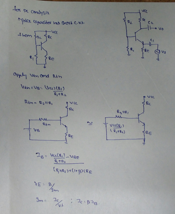
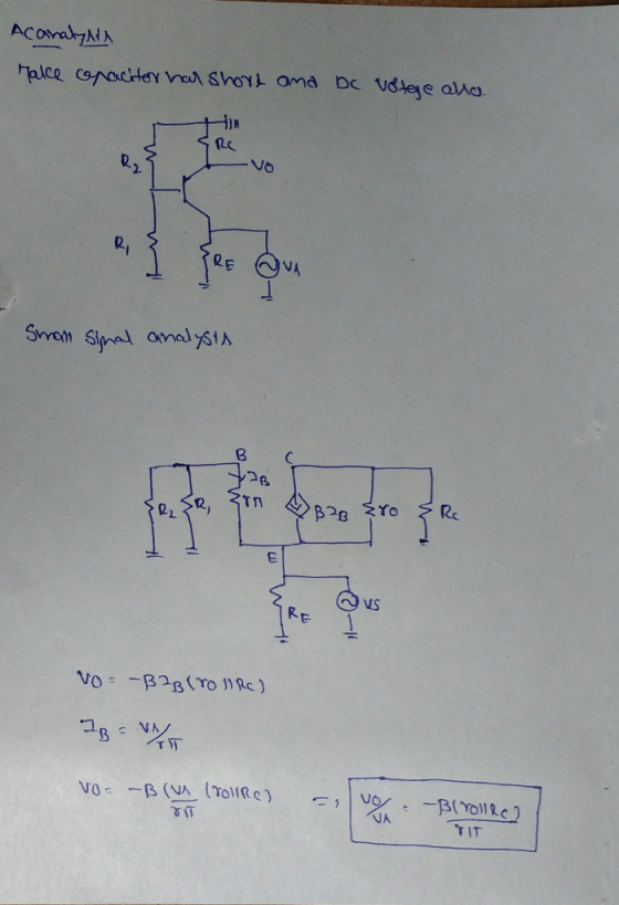
FIND THE VALUES OF Rb1, Rb2, Re,Rc, rin , rout, overall gain and open circuit gain First, design a common emitter BJT a...
 FIND THE VALUES OF Rb1, Rb2, Re,Rc, rin , rout, overall gain and
open circuit gain
First, design a common emitter BJT amplifier Second, analyze the amplifier.( Avo, Gv, Rin, Rout) Third, compare your calculation with Multisim. Report must include comparison between your calculation & simulation results overall voltage gain, open circuit voltage gain, input resistance, and output resistance. This design project is not group work, must be done individually. Type your report. Design a discrete common emitter BJT amplifier.(Determine...
FIND THE VALUES OF Rb1, Rb2, Re,Rc, rin , rout, overall gain and
open circuit gain
First, design a common emitter BJT amplifier Second, analyze the amplifier.( Avo, Gv, Rin, Rout) Third, compare your calculation with Multisim. Report must include comparison between your calculation & simulation results overall voltage gain, open circuit voltage gain, input resistance, and output resistance. This design project is not group work, must be done individually. Type your report. Design a discrete common emitter BJT amplifier.(Determine...
Please answer clearly 2. Consider the circuit shown in Figure 1. Determine values of Ri, R2, and Rc to provide the quie...
 Please answer clearly
2. Consider the circuit shown in Figure 1. Determine values of Ri, R2, and Rc to provide the quiescent emitter current 1.5 mA and the quiescent collector to emitter voltage 5V. Assume β 100, Re-I㏀、Va= 200V, VBEon-0.7V, and VT= 25mV. R1 Rc Vcc に 10v R2 Re Figure 1: BJT biasing configuration
2. Consider the circuit shown in Figure 1. Determine values of Ri, R2, and Rc to provide the quiescent emitter current 1.5 mA and the...
Please answer clearly
2. Consider the circuit shown in Figure 1. Determine values of Ri, R2, and Rc to provide the quiescent emitter current 1.5 mA and the quiescent collector to emitter voltage 5V. Assume β 100, Re-I㏀、Va= 200V, VBEon-0.7V, and VT= 25mV. R1 Rc Vcc に 10v R2 Re Figure 1: BJT biasing configuration
2. Consider the circuit shown in Figure 1. Determine values of Ri, R2, and Rc to provide the quiescent emitter current 1.5 mA and the...
4. Design a npn BJT C-E amplifier circuit for the following specifications and given values: Voltage...
 4. Design a npn BJT C-E amplifier circuit for the following specifications and given values: Voltage Gain Input resistance Load resistance Supply voltage Av = -60 Ri = 5k92 RL = 6k2 Vcc= 16V Assume Re is fully bypassed. The input source internal resistance Rs = 0.12. B=120 and VBE= 0.65V. Draw the actual circuit and its ac equivalent circuit
Fundamentals of Electronic Engineering Answer should be step by step and readable (clear handwriting) Given: •...
 Fundamentals of Electronic Engineering
Answer should be step by step and readable (clear
handwriting)
Given: • Power voltage: • Collector resistor: • Current amplification of BJT: • Source peak voltage: • Input/Output resistance: • The corner frequency: Vcc = 12V; Rc = 4k22; B = 100; Vs = 10mV; Rvs, RL = 1 ks2; f-3dB = 100Hz. Vec=12V w • Rc www R1 HE Сс CC2 RL + R2 RE CE Find: ? Bias quiescent point: Load line, Q-point, VcEQ,...
Fundamentals of Electronic Engineering
Answer should be step by step and readable (clear
handwriting)
Given: • Power voltage: • Collector resistor: • Current amplification of BJT: • Source peak voltage: • Input/Output resistance: • The corner frequency: Vcc = 12V; Rc = 4k22; B = 100; Vs = 10mV; Rvs, RL = 1 ks2; f-3dB = 100Hz. Vec=12V w • Rc www R1 HE Сс CC2 RL + R2 RE CE Find: ? Bias quiescent point: Load line, Q-point, VcEQ,...
Avec Úvo SRE L V II. (5pt) Consider the above-right common-collector or emitter-follower BJT amplifier circuit....
 Avec Úvo SRE L V II. (5pt) Consider the above-right common-collector or emitter-follower BJT amplifier circuit. Given: ß= 100, RE = 10 k1, Vcc = 20 V, RB = 5 k1, R1 = 10 kl, and Ry = 2 k1. (a) (1pt) Find the Q-point, i.e. Ibo, Ico, and VCEO; (b) (1pt) draw the small-signal equivalent circuit assuming that the capacitors (C, and Cy) are short circuits for the small signal; (c) (1pt) solve for the voltage gain, Av; (d)...
x=4 Question 3: The parameters of both bjt are as follows: base emitter turn on voltage...
 x=4
Question 3: The parameters of both bjt are as follows: base emitter turn on voltage is VBE,ON = 0.7 V, early voltage VA = 0, ac current gain B = 99. Small signal ac voltage source viis applied to the base of Q1 through a large capacitor. The resistors on the left branch are 63 X and 37xX2 (63 times X and 37 times X, note that these are not k2!!!). The remaining resistors are 4 k 2, 3...
x=4
Question 3: The parameters of both bjt are as follows: base emitter turn on voltage is VBE,ON = 0.7 V, early voltage VA = 0, ac current gain B = 99. Small signal ac voltage source viis applied to the base of Q1 through a large capacitor. The resistors on the left branch are 63 X and 37xX2 (63 times X and 37 times X, note that these are not k2!!!). The remaining resistors are 4 k 2, 3...
1. Consider the Common-Emitter BJT amplifier circuit, shown below. VD VOD BJT Parameters: B=99 A/A i=0...
 1. Consider the Common-Emitter BJT amplifier circuit, shown below. VD VOD BJT Parameters: B=99 A/A i=0 RE Co Circuit Parameters: Ca Cc2 = 0 F Car = OF R = 2022 R = 2002 R1 = 25.8 k22 Ry2 = 51.6 ks V = 15 V VEE=0 V Сct Active Mode: Va >0.2 V Vwx=0.7V Ic=B1, Ic=al, 1 R2 3 SRCA a) Find the open-circuit voltage gain, Ave, of this amplifier circuit. Verify your assumptions. b) Compute the input resistance,...
Can I get help with part g through part r, please? Given the following Common-Emitter Amplifier...
 Can I get help with part g through part r, please?
Given the following Common-Emitter Amplifier with Voltage-Divider Bias: The transistor is a Silicon device with B160 (Beta 160) and transistor r.= 30 kn: 20 V 34.7k LAL = Vou 35.10 31.1k LRE $3900 03 - Find the following quantities in parts a through where means Quiescent DC): a) Thevenin Voltage and Thevenin Resistance Re b) Base Current la Collector Current le d) Emitter Current le e) Transistor Collector-Emitter Quiescent...
Can I get help with part g through part r, please?
Given the following Common-Emitter Amplifier with Voltage-Divider Bias: The transistor is a Silicon device with B160 (Beta 160) and transistor r.= 30 kn: 20 V 34.7k LAL = Vou 35.10 31.1k LRE $3900 03 - Find the following quantities in parts a through where means Quiescent DC): a) Thevenin Voltage and Thevenin Resistance Re b) Base Current la Collector Current le d) Emitter Current le e) Transistor Collector-Emitter Quiescent...
Consider the npn BJT with a turn-on voltage V1 = 0.70 V, and a saturation emitter-collector...
 Consider the npn BJT with a turn-on voltage V1 = 0.70 V, and a saturation emitter-collector voltage V CE/SAT) = 0.20 V. (a) [20 points) Consider this transistor in a common- emitter circuit (Re = 0). Design this common- emitter circuit to produce the IV (Ic vs. VCE) characteristic and load line (LL) as shown in the graph. Your answers are the following: a drawing of the circuit; the values of Vcc, Rc, VBB, and Ra; and the value for...
Please explain part A in details thx! Question 3 An n'pn Si BJT is shown in Figure Q3(a). The emitter is heavily doped with 1020 cm3 whereas the base and collector are lightly doped with 5x10¹⁸ a...
 Please explain part A in details thx!
Question 3 An n'pn Si BJT is shown in Figure Q3(a). The emitter is heavily doped with 1020 cm3 whereas the base and collector are lightly doped with 5x10¹⁸ and 3x10¹⁸, respectively. The lengths of emitter, base, and collector are 0.5um, 0.2um, and 0.5 um.. The dielectric constant of silicon is 11.8 and the intrinsic carrier concentration at 300 K is 1.5x1010 cm3. Assume that a 0.026 eV at 300 K. 0.99, e...
Please explain part A in details thx!
Question 3 An n'pn Si BJT is shown in Figure Q3(a). The emitter is heavily doped with 1020 cm3 whereas the base and collector are lightly doped with 5x10¹⁸ and 3x10¹⁸, respectively. The lengths of emitter, base, and collector are 0.5um, 0.2um, and 0.5 um.. The dielectric constant of silicon is 11.8 and the intrinsic carrier concentration at 300 K is 1.5x1010 cm3. Assume that a 0.026 eV at 300 K. 0.99, e...
 FIND THE VALUES OF Rb1, Rb2, Re,Rc, rin , rout, overall gain and
open circuit gain
First, design a common emitter BJT amplifier Second, analyze the amplifier.( Avo, Gv, Rin, Rout) Third, compare your calculation with Multisim. Report must include comparison between your calculation & simulation results overall voltage gain, open circuit voltage gain, input resistance, and output resistance. This design project is not group work, must be done individually. Type your report. Design a discrete common emitter BJT amplifier.(Determine...
FIND THE VALUES OF Rb1, Rb2, Re,Rc, rin , rout, overall gain and
open circuit gain
First, design a common emitter BJT amplifier Second, analyze the amplifier.( Avo, Gv, Rin, Rout) Third, compare your calculation with Multisim. Report must include comparison between your calculation & simulation results overall voltage gain, open circuit voltage gain, input resistance, and output resistance. This design project is not group work, must be done individually. Type your report. Design a discrete common emitter BJT amplifier.(Determine...
 Please answer clearly
2. Consider the circuit shown in Figure 1. Determine values of Ri, R2, and Rc to provide the quiescent emitter current 1.5 mA and the quiescent collector to emitter voltage 5V. Assume β 100, Re-I㏀、Va= 200V, VBEon-0.7V, and VT= 25mV. R1 Rc Vcc に 10v R2 Re Figure 1: BJT biasing configuration
2. Consider the circuit shown in Figure 1. Determine values of Ri, R2, and Rc to provide the quiescent emitter current 1.5 mA and the...
Please answer clearly
2. Consider the circuit shown in Figure 1. Determine values of Ri, R2, and Rc to provide the quiescent emitter current 1.5 mA and the quiescent collector to emitter voltage 5V. Assume β 100, Re-I㏀、Va= 200V, VBEon-0.7V, and VT= 25mV. R1 Rc Vcc に 10v R2 Re Figure 1: BJT biasing configuration
2. Consider the circuit shown in Figure 1. Determine values of Ri, R2, and Rc to provide the quiescent emitter current 1.5 mA and the...
 4. Design a npn BJT C-E amplifier circuit for the following specifications and given values: Voltage Gain Input resistance Load resistance Supply voltage Av = -60 Ri = 5k92 RL = 6k2 Vcc= 16V Assume Re is fully bypassed. The input source internal resistance Rs = 0.12. B=120 and VBE= 0.65V. Draw the actual circuit and its ac equivalent circuit
 Fundamentals of Electronic Engineering
Answer should be step by step and readable (clear
handwriting)
Given: • Power voltage: • Collector resistor: • Current amplification of BJT: • Source peak voltage: • Input/Output resistance: • The corner frequency: Vcc = 12V; Rc = 4k22; B = 100; Vs = 10mV; Rvs, RL = 1 ks2; f-3dB = 100Hz. Vec=12V w • Rc www R1 HE Сс CC2 RL + R2 RE CE Find: ? Bias quiescent point: Load line, Q-point, VcEQ,...
Fundamentals of Electronic Engineering
Answer should be step by step and readable (clear
handwriting)
Given: • Power voltage: • Collector resistor: • Current amplification of BJT: • Source peak voltage: • Input/Output resistance: • The corner frequency: Vcc = 12V; Rc = 4k22; B = 100; Vs = 10mV; Rvs, RL = 1 ks2; f-3dB = 100Hz. Vec=12V w • Rc www R1 HE Сс CC2 RL + R2 RE CE Find: ? Bias quiescent point: Load line, Q-point, VcEQ,...
 Avec Úvo SRE L V II. (5pt) Consider the above-right common-collector or emitter-follower BJT amplifier circuit. Given: ß= 100, RE = 10 k1, Vcc = 20 V, RB = 5 k1, R1 = 10 kl, and Ry = 2 k1. (a) (1pt) Find the Q-point, i.e. Ibo, Ico, and VCEO; (b) (1pt) draw the small-signal equivalent circuit assuming that the capacitors (C, and Cy) are short circuits for the small signal; (c) (1pt) solve for the voltage gain, Av; (d)...
 x=4
Question 3: The parameters of both bjt are as follows: base emitter turn on voltage is VBE,ON = 0.7 V, early voltage VA = 0, ac current gain B = 99. Small signal ac voltage source viis applied to the base of Q1 through a large capacitor. The resistors on the left branch are 63 X and 37xX2 (63 times X and 37 times X, note that these are not k2!!!). The remaining resistors are 4 k 2, 3...
x=4
Question 3: The parameters of both bjt are as follows: base emitter turn on voltage is VBE,ON = 0.7 V, early voltage VA = 0, ac current gain B = 99. Small signal ac voltage source viis applied to the base of Q1 through a large capacitor. The resistors on the left branch are 63 X and 37xX2 (63 times X and 37 times X, note that these are not k2!!!). The remaining resistors are 4 k 2, 3...
 1. Consider the Common-Emitter BJT amplifier circuit, shown below. VD VOD BJT Parameters: B=99 A/A i=0 RE Co Circuit Parameters: Ca Cc2 = 0 F Car = OF R = 2022 R = 2002 R1 = 25.8 k22 Ry2 = 51.6 ks V = 15 V VEE=0 V Сct Active Mode: Va >0.2 V Vwx=0.7V Ic=B1, Ic=al, 1 R2 3 SRCA a) Find the open-circuit voltage gain, Ave, of this amplifier circuit. Verify your assumptions. b) Compute the input resistance,...
 Can I get help with part g through part r, please?
Given the following Common-Emitter Amplifier with Voltage-Divider Bias: The transistor is a Silicon device with B160 (Beta 160) and transistor r.= 30 kn: 20 V 34.7k LAL = Vou 35.10 31.1k LRE $3900 03 - Find the following quantities in parts a through where means Quiescent DC): a) Thevenin Voltage and Thevenin Resistance Re b) Base Current la Collector Current le d) Emitter Current le e) Transistor Collector-Emitter Quiescent...
Can I get help with part g through part r, please?
Given the following Common-Emitter Amplifier with Voltage-Divider Bias: The transistor is a Silicon device with B160 (Beta 160) and transistor r.= 30 kn: 20 V 34.7k LAL = Vou 35.10 31.1k LRE $3900 03 - Find the following quantities in parts a through where means Quiescent DC): a) Thevenin Voltage and Thevenin Resistance Re b) Base Current la Collector Current le d) Emitter Current le e) Transistor Collector-Emitter Quiescent...
 Consider the npn BJT with a turn-on voltage V1 = 0.70 V, and a saturation emitter-collector voltage V CE/SAT) = 0.20 V. (a) [20 points) Consider this transistor in a common- emitter circuit (Re = 0). Design this common- emitter circuit to produce the IV (Ic vs. VCE) characteristic and load line (LL) as shown in the graph. Your answers are the following: a drawing of the circuit; the values of Vcc, Rc, VBB, and Ra; and the value for...
 Please explain part A in details thx!
Question 3 An n'pn Si BJT is shown in Figure Q3(a). The emitter is heavily doped with 1020 cm3 whereas the base and collector are lightly doped with 5x10¹⁸ and 3x10¹⁸, respectively. The lengths of emitter, base, and collector are 0.5um, 0.2um, and 0.5 um.. The dielectric constant of silicon is 11.8 and the intrinsic carrier concentration at 300 K is 1.5x1010 cm3. Assume that a 0.026 eV at 300 K. 0.99, e...
Please explain part A in details thx!
Question 3 An n'pn Si BJT is shown in Figure Q3(a). The emitter is heavily doped with 1020 cm3 whereas the base and collector are lightly doped with 5x10¹⁸ and 3x10¹⁸, respectively. The lengths of emitter, base, and collector are 0.5um, 0.2um, and 0.5 um.. The dielectric constant of silicon is 11.8 and the intrinsic carrier concentration at 300 K is 1.5x1010 cm3. Assume that a 0.026 eV at 300 K. 0.99, e...
Most questions answered within 3 hours.
-
Where is the error in this code sequence?
String s1 = "Hello";
String s2 = "ello";...
asked 11 months ago -
Financial data for Joel de Paris, Inc., for last year
follow:
Joel de Paris, Inc.
Balance...
asked 11 months ago -
Consider this reaction:
Al2(SO4)3 (aq)+ BaCl3
(aq) Al2Cl6 (aq)- +
3BaSO4(s) . What is the...
asked 11 months ago -
Suppose that Savneet is considering increasing her
recent random sample from 20 car rentals to 40...
asked 11 months ago -
Trucks arrive at an unloading terminal at an average rate of 120
per hour.
Trucks arrive...
asked 11 months ago -
Why are methanol and ethanol completely soluble in water while
octanol is not very little soluble....
asked 11 months ago -
A facilities manager at a university reads in a research report
that the mean amount of...
asked 11 months ago -
When the CuSO4 is rehydrated by adding water to the anhydrous
compound, is this an endothermic...
asked 11 months ago -
A ray of sunlight is passing from diamond into crown glass; the
angle of incidence is...
asked 11 months ago -
A block of mass 0.249 kg is placed on top of a light, vertical
spring of...
asked 11 months ago -
how do the kidneys compensate in the presences of acidosis
a) trigger hyperventilate
b) reserve acid...
asked 11 months ago -
Question 501 pts
The rental rate of capital to the firm increases. Which of the
following...
asked 11 months ago