

Homework Answers
Hey there! Hope the solution is clear. Thank you and all the
very best :)


![Input impedance Zin - I hie - | here life RL (1 + use Re] (Answe pulting the values, we get Zin = 1000 - 10-4 x 100, 2000 1 +](http://img.homeworklib.com/questions/c91cd3c0-d210-11ea-af40-7bf7e0bfa700.png?x-oss-process=image/resize,w_560)
Add Answer to:
Q1(a) [5 Marks The diagram of Fig Ql(a) below describes how a Bipolar Junction Transistor (BJT)...
2. (36% ) In Fig. 2, the device parameters and (W/L) ratios for Q1-Q3 are given...
 2. (36% ) In Fig. 2, the device parameters and (W/L) ratios for Q1-Q3 are given below (WIL), 2 (W/L)2-2 (W/L); (a) (10%) If IREF-2nA, find VD3 and VS3 and verify if Q3 is in saturation. Ignore the channel length modulation for DC analysis. Note: DC Vc30 (b) (12%) Draw the "small signal" circuit for the complete +10 V amplifier. Based on the circuit, derive the AC voltage gain vo/vi in terms gm, ro and RD (please use appropriate subscripts...
pls answer all and asap.tqvm. (a) () What is the significant used of multistage amplifier compared...
 pls
answer all and asap.tqvm.
(a) () What is the significant used of multistage amplifier compared to single stage amplifier? (2 marks) (ii) In terms of circuit connection, how to differentiate between direct and capacitively coupled amplifier circuit? (1 mark) (ii) Give a reason why the capacitively coupled amplifier circuit is not suitable for amplifying DC voltage? (2 marks) (b) The multistage amplifier circuit of Figure Q.3 have the following parameters: Q1, Q2: B = 200, VBE = 0.7 V,....
pls
answer all and asap.tqvm.
(a) () What is the significant used of multistage amplifier compared to single stage amplifier? (2 marks) (ii) In terms of circuit connection, how to differentiate between direct and capacitively coupled amplifier circuit? (1 mark) (ii) Give a reason why the capacitively coupled amplifier circuit is not suitable for amplifying DC voltage? (2 marks) (b) The multistage amplifier circuit of Figure Q.3 have the following parameters: Q1, Q2: B = 200, VBE = 0.7 V,....
This is the solution to a homework problem. The table below was completely unfilled. I don't understand some of the filled in cells. If possible please show the circuit diagram to solve this and t...
 This is the solution to a homework problem. The table below was
completely unfilled. I don't understand some of the filled in
cells. If possible please show the circuit diagram to solve this
and the relationships between the given parameters. In order to
fill in the table, you would need a small signal model and a DC
model. From the two models you get the equations you need to fill
in the cells in the table. This solution was provided...
This is the solution to a homework problem. The table below was
completely unfilled. I don't understand some of the filled in
cells. If possible please show the circuit diagram to solve this
and the relationships between the given parameters. In order to
fill in the table, you would need a small signal model and a DC
model. From the two models you get the equations you need to fill
in the cells in the table. This solution was provided...
For the amplifier configuration in Figure 4.1, the transistor parameters are; loss 10 mA, Vp 5...
 For the amplifier configuration in Figure 4.1, the transistor parameters are; loss 10 mA, Vp 5 V and 0.01 V. The circuit parameters are; VDo 12 V, Rs 1.2 kn, Ri-265 k, R2 165 k, and RL-0.5 k [Bagi tatarajah penguat dalam Rajah 4.1, parameter transistor adalah; Inss 10 m, V- sV dan à-0.01 Parameter litar adalah; V 12 V, Rs 1.2 k R 265 R-165 k, dan R-0.5 ko VDD Rin R Ro Cc Cc2 RL R2 Rs +...
Problem #5 (20 points) n the two stage cascade amplifier circuit shown below, the MOSFET has...
 Problem #5 (20 points) n the two stage cascade amplifier circuit shown below, the MOSFET has V IV and k-0s mA/ and the BIT has p 100 a) Perform the DC analysis of this circuit and based on the appropriate DC current values, calculate the small signal parameters for each transistor. b) Replace each transistor with its appropriate small signal model (neglecting ro) and draw the resulting smali- signal circuit for this amplifier circuit. HINT: You may use the T-model...
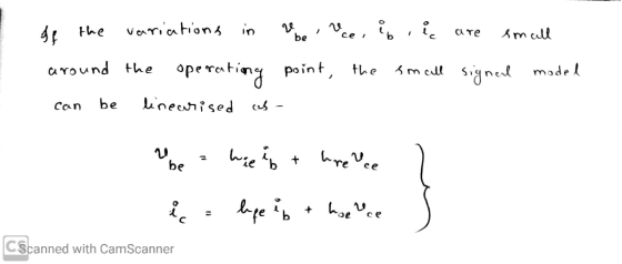
Question 4 (25 Marks) (5) 1. Derive the Dynamic Emitter Resistance, re that is used in...
 Question 4 (25 Marks) (5) 1. Derive the Dynamic Emitter Resistance, re that is used in the re-model small-signal analysis of BJT. 2. The circuit in Figure 7 shows the multistage cascade of two single transistors with B=100. Given the value of Vpp=12 V, R1=120 kN, R2=40 kN, R3=100 ks, Ra=30 kn, RE1=3.9 kN, Rez=4.5 kN, Rc1=6.5 kN, Rc2=8 ks, (2) (4) (a) Identify the transistor configuration for all stages. (b) Determine the d.c collector current (Ici and I cz)...
Lab Preparation . Using DC analysis, and assuming that the transistors (QuEr and Q) are in...
 Lab Preparation . Using DC analysis, and assuming that the transistors (QuEr and Q) are in the active mode, determine the value of RREF required for generating a copy current of 0.755 mA. Take the value of Vcc to be 8 V, and the value of VE in the active mode to be equal to 0.7V. Vee H Qur о RaI Figure 3 Single-stage amplifier biased by a simple current miror device 2. The circuit shown in Figure 3, is...
An analogue amplifier circuit is shown in Figure 1 below. VDD Q5 15V JL - Vout...
 An analogue amplifier circuit is shown in Figure 1 below. VDD Q5 15V JL - Vout Irer RI Vina JET T7T Figure 1 Integrated amplifier circuit. Circuit Data: Vpp = 15 V, IREF = I1 = I2 = 1.0 mA Transistor Data: Q1: NMOS, un Cox = 80 A/V?, W/L = 100 um/0.8 um, Vtn = 0.8 V, L = 0.10 um/V Q2: NPN BJT, B = 100, Vbe = 0.7 V, VA = 150 V Q3, Q4: NMOS, un...
Question 1 In the diagram of Superheterodne AM receiver shown below explain the function of each block. (a) 15 marks Antenna Speaker Audio and power amplifiers RF IF Mixer Detector Mi amplifier a...
 Question 1 In the diagram of Superheterodne AM receiver shown below explain the function of each block. (a) 15 marks Antenna Speaker Audio and power amplifiers RF IF Mixer Detector Mi amplifier amplifier AGC --_Local Gang tuned oscillator (b) For a 4-bit DAC, calculate the output voltage for an input code word 1010 if a [10 marks] logic 1 is 10V and a logic 0 is 0V, and R = RFI kΩ Total: 25 marks] Question 2 (a) Explain the...
 2. (36% ) In Fig. 2, the device parameters and (W/L) ratios for Q1-Q3 are given below (WIL), 2 (W/L)2-2 (W/L); (a) (10%) If IREF-2nA, find VD3 and VS3 and verify if Q3 is in saturation. Ignore the channel length modulation for DC analysis. Note: DC Vc30 (b) (12%) Draw the "small signal" circuit for the complete +10 V amplifier. Based on the circuit, derive the AC voltage gain vo/vi in terms gm, ro and RD (please use appropriate subscripts...
 pls
answer all and asap.tqvm.
(a) () What is the significant used of multistage amplifier compared to single stage amplifier? (2 marks) (ii) In terms of circuit connection, how to differentiate between direct and capacitively coupled amplifier circuit? (1 mark) (ii) Give a reason why the capacitively coupled amplifier circuit is not suitable for amplifying DC voltage? (2 marks) (b) The multistage amplifier circuit of Figure Q.3 have the following parameters: Q1, Q2: B = 200, VBE = 0.7 V,....
pls
answer all and asap.tqvm.
(a) () What is the significant used of multistage amplifier compared to single stage amplifier? (2 marks) (ii) In terms of circuit connection, how to differentiate between direct and capacitively coupled amplifier circuit? (1 mark) (ii) Give a reason why the capacitively coupled amplifier circuit is not suitable for amplifying DC voltage? (2 marks) (b) The multistage amplifier circuit of Figure Q.3 have the following parameters: Q1, Q2: B = 200, VBE = 0.7 V,....
 This is the solution to a homework problem. The table below was
completely unfilled. I don't understand some of the filled in
cells. If possible please show the circuit diagram to solve this
and the relationships between the given parameters. In order to
fill in the table, you would need a small signal model and a DC
model. From the two models you get the equations you need to fill
in the cells in the table. This solution was provided...
This is the solution to a homework problem. The table below was
completely unfilled. I don't understand some of the filled in
cells. If possible please show the circuit diagram to solve this
and the relationships between the given parameters. In order to
fill in the table, you would need a small signal model and a DC
model. From the two models you get the equations you need to fill
in the cells in the table. This solution was provided...
 For the amplifier configuration in Figure 4.1, the transistor parameters are; loss 10 mA, Vp 5 V and 0.01 V. The circuit parameters are; VDo 12 V, Rs 1.2 kn, Ri-265 k, R2 165 k, and RL-0.5 k [Bagi tatarajah penguat dalam Rajah 4.1, parameter transistor adalah; Inss 10 m, V- sV dan à-0.01 Parameter litar adalah; V 12 V, Rs 1.2 k R 265 R-165 k, dan R-0.5 ko VDD Rin R Ro Cc Cc2 RL R2 Rs +...
 Problem #5 (20 points) n the two stage cascade amplifier circuit shown below, the MOSFET has V IV and k-0s mA/ and the BIT has p 100 a) Perform the DC analysis of this circuit and based on the appropriate DC current values, calculate the small signal parameters for each transistor. b) Replace each transistor with its appropriate small signal model (neglecting ro) and draw the resulting smali- signal circuit for this amplifier circuit. HINT: You may use the T-model...
 Question 4 (25 Marks) (5) 1. Derive the Dynamic Emitter Resistance, re that is used in the re-model small-signal analysis of BJT. 2. The circuit in Figure 7 shows the multistage cascade of two single transistors with B=100. Given the value of Vpp=12 V, R1=120 kN, R2=40 kN, R3=100 ks, Ra=30 kn, RE1=3.9 kN, Rez=4.5 kN, Rc1=6.5 kN, Rc2=8 ks, (2) (4) (a) Identify the transistor configuration for all stages. (b) Determine the d.c collector current (Ici and I cz)...
 Lab Preparation . Using DC analysis, and assuming that the transistors (QuEr and Q) are in the active mode, determine the value of RREF required for generating a copy current of 0.755 mA. Take the value of Vcc to be 8 V, and the value of VE in the active mode to be equal to 0.7V. Vee H Qur о RaI Figure 3 Single-stage amplifier biased by a simple current miror device 2. The circuit shown in Figure 3, is...
 An analogue amplifier circuit is shown in Figure 1 below. VDD Q5 15V JL - Vout Irer RI Vina JET T7T Figure 1 Integrated amplifier circuit. Circuit Data: Vpp = 15 V, IREF = I1 = I2 = 1.0 mA Transistor Data: Q1: NMOS, un Cox = 80 A/V?, W/L = 100 um/0.8 um, Vtn = 0.8 V, L = 0.10 um/V Q2: NPN BJT, B = 100, Vbe = 0.7 V, VA = 150 V Q3, Q4: NMOS, un...
 Question 1 In the diagram of Superheterodne AM receiver shown below explain the function of each block. (a) 15 marks Antenna Speaker Audio and power amplifiers RF IF Mixer Detector Mi amplifier amplifier AGC --_Local Gang tuned oscillator (b) For a 4-bit DAC, calculate the output voltage for an input code word 1010 if a [10 marks] logic 1 is 10V and a logic 0 is 0V, and R = RFI kΩ Total: 25 marks] Question 2 (a) Explain the...
Most questions answered within 3 hours.
-
Where is the error in this code sequence?
String s1 = "Hello";
String s2 = "ello";...
asked 11 months ago -
Financial data for Joel de Paris, Inc., for last year
follow:
Joel de Paris, Inc.
Balance...
asked 11 months ago -
Consider this reaction:
Al2(SO4)3 (aq)+ BaCl3
(aq) Al2Cl6 (aq)- +
3BaSO4(s) . What is the...
asked 11 months ago -
Suppose that Savneet is considering increasing her
recent random sample from 20 car rentals to 40...
asked 11 months ago -
Trucks arrive at an unloading terminal at an average rate of 120
per hour.
Trucks arrive...
asked 11 months ago -
Why are methanol and ethanol completely soluble in water while
octanol is not very little soluble....
asked 11 months ago -
A facilities manager at a university reads in a research report
that the mean amount of...
asked 11 months ago -
When the CuSO4 is rehydrated by adding water to the anhydrous
compound, is this an endothermic...
asked 11 months ago -
A ray of sunlight is passing from diamond into crown glass; the
angle of incidence is...
asked 11 months ago -
A block of mass 0.249 kg is placed on top of a light, vertical
spring of...
asked 11 months ago -
how do the kidneys compensate in the presences of acidosis
a) trigger hyperventilate
b) reserve acid...
asked 11 months ago -
Question 501 pts
The rental rate of capital to the firm increases. Which of the
following...
asked 11 months ago