
Homework Answers
Add Answer to:
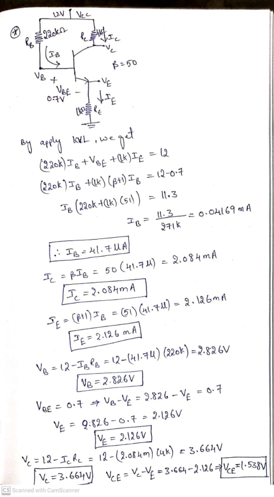
5 نقاط For the circuit shown, If there is an added 1 K. Ohm resistor at...
Problem 5 Given the following circuit, assume the following parameters VBB IV, RB 220 k, RC...
 Problem 5 Given the following circuit, assume the following parameters VBB IV, RB 220 k, RC = 2 k, VCC= 10 V, VBE(on)-0.7 V, and B 200 a) Calculate the base, collector, and emitter currents and the C-E voltage, also, calculate the transistor power dissipation b) What transistor configuration does the circuit resemble? Vcc=10V RC=2k Rg=220 kQ VCE VBB= 1V o + VRE IB
please choose one of the answer choices above. Must show all work, thank you Question 1...
 please choose one of the answer choices above.
Must show all work, thank you
Question 1 CIRCUIT A.1 (2.5 Marks) + Vcc RB IB Rc Vc VB Fig. 1: CIRCUIT A.1 Statement: Sketching relevant output (Vc-Ic) characteristics decide on Q-point coordinates and DC load-line details: That is, determine DC operating conditions of the NPN-BJT/Si circuit of Fig.1 (denoting the type Circuit A1). Assume the following: Vcc= 12 volt; Rc = 3.6 k; RB = 500 k and a = 0.9....
please choose one of the answer choices above.
Must show all work, thank you
Question 1 CIRCUIT A.1 (2.5 Marks) + Vcc RB IB Rc Vc VB Fig. 1: CIRCUIT A.1 Statement: Sketching relevant output (Vc-Ic) characteristics decide on Q-point coordinates and DC load-line details: That is, determine DC operating conditions of the NPN-BJT/Si circuit of Fig.1 (denoting the type Circuit A1). Assume the following: Vcc= 12 volt; Rc = 3.6 k; RB = 500 k and a = 0.9....
please choose one of the answer choices above. Must show all work, thank you Question 4...
 please choose one of the answer choices above.
Must show all work, thank you
Question 4 CIRCUIT B2 (2.5 Marks) +Vcc Rc IRC Vic RB Ів Vc VB VE RE IE FIG.4: CIRCUIT B2 Statement: Sketching relevant output (Vc-Ic) characteristics decide on Q-point coordinates and DC load-line details: That is, determine DC operating conditions of the NPN-BJT/Si circuit of Fig.4 (denoting the type Circuit B2). Assume the following: Vcc= 24 volt; Rc = 5.0 k; RE = 1000 ohm; RB...
please choose one of the answer choices above.
Must show all work, thank you
Question 4 CIRCUIT B2 (2.5 Marks) +Vcc Rc IRC Vic RB Ів Vc VB VE RE IE FIG.4: CIRCUIT B2 Statement: Sketching relevant output (Vc-Ic) characteristics decide on Q-point coordinates and DC load-line details: That is, determine DC operating conditions of the NPN-BJT/Si circuit of Fig.4 (denoting the type Circuit B2). Assume the following: Vcc= 24 volt; Rc = 5.0 k; RE = 1000 ohm; RB...
It Kind of goes without saying but if you have no knowledge than dont comment or try and answer this question you dope Questions 1-3 below are about the amplifier circuit of Figure 1. Here Vcc is a...
 It
Kind of goes without saying but if you have no knowledge than dont
comment or try and answer this question you dope
Questions 1-3 below are about the amplifier circuit of Figure 1. Here Vcc is a fixed voltage The base voltage vB(t) is time-varying, and is of the form vB(t) V(t) where VB is a DC offset, and vb(t) is a time-varying purely AC signal. Suppose the amplitude of vb is A. Assume that the capacitor C is...
It
Kind of goes without saying but if you have no knowledge than dont
comment or try and answer this question you dope
Questions 1-3 below are about the amplifier circuit of Figure 1. Here Vcc is a fixed voltage The base voltage vB(t) is time-varying, and is of the form vB(t) V(t) where VB is a DC offset, and vb(t) is a time-varying purely AC signal. Suppose the amplitude of vb is A. Assume that the capacitor C is...
please choose one of the answer choices above. Must show all work, thank you Question 2...
 please choose one of the answer choices above.
Must show all work, thank you
Question 2 CIRCUIT A2 (2.5 Marks) + Ver Rc Ic с IR Fig. 2: CIRCUIT A.2 Statement: Sketching relevant output (Vc-Ic) characteristics decide on Q-point coordinates and DC load-line details: That is, determine DC operating conditions of the NPN-BJT/Si circuit of Fig.2 (denoting the type Circuit A2). Assume the following: Vcc= 24 volt; Rc = 5.0 k; RB = 1500 k and B = 125. Required...
please choose one of the answer choices above.
Must show all work, thank you
Question 2 CIRCUIT A2 (2.5 Marks) + Ver Rc Ic с IR Fig. 2: CIRCUIT A.2 Statement: Sketching relevant output (Vc-Ic) characteristics decide on Q-point coordinates and DC load-line details: That is, determine DC operating conditions of the NPN-BJT/Si circuit of Fig.2 (denoting the type Circuit A2). Assume the following: Vcc= 24 volt; Rc = 5.0 k; RB = 1500 k and B = 125. Required...
4. Lab VIII: Experiment VII The Bipolar Junction Transistor (BJT) Characteristics The bipolar junction transistor (BJT)...
 4. Lab VIII: Experiment VII The Bipolar Junction Transistor (BJT) Characteristics The bipolar junction transistor (BJT) is a three-terminal solid state device widely used as an amplifier (or switching) device. It consists of two n-type materials sandwiched by p-type material (npn) or two p-type and n-type. The terminals (sections) are known as emitter E, base B and collector C. Two currents and two voltages uniquely describe the behavior of the device. The third current/voltage can be determined through KCL/KVL. See...
Experiment 2: Good biasing Set up the circuit with R2 12 k2, R RE 1 k, and Vcc 15 V 39 k2, Rc = 2 k?. Circuit An...
 Experiment 2: Good biasing Set up the circuit with R2 12 k2, R RE 1 k, and Vcc 15 V 39 k2, Rc = 2 k?. Circuit Analysis: Compute Ic, I, and VCE PSpice Simulation: a) Simulate the circuit with PSpice (bias point details only) and compare values of Ic, IB, VCE, and VBE from PSpice simulations with your analytical calculations. b) Rerun your PSpice simulations for temperatures of 0 and 60°C. Make a table of Ic IB, VCE, and...
please choose one of the answer choices above. Must show all work, thank you Question 3...
 please choose one of the answer choices above.
Must show all work, thank you
Question 3 CIRCUIT B1 (2.5 Marks) + Vcc Rc IRC > IC RB Ів + VCE IE FIG. 3: CIRCUIT B1 Statement: Sketching relevant output (Vc-Ic) characteristics decide on Q-point coordinates and DC load-line details: That is, determine DC operating conditions of the NPN-BJT/Si circuit of Fig.3 (denoting the type Circuit B1). Assume the following: Vcc= 20 volt; Rc = 2.5 k; RB = 350 k...
please choose one of the answer choices above.
Must show all work, thank you
Question 3 CIRCUIT B1 (2.5 Marks) + Vcc Rc IRC > IC RB Ів + VCE IE FIG. 3: CIRCUIT B1 Statement: Sketching relevant output (Vc-Ic) characteristics decide on Q-point coordinates and DC load-line details: That is, determine DC operating conditions of the NPN-BJT/Si circuit of Fig.3 (denoting the type Circuit B1). Assume the following: Vcc= 20 volt; Rc = 2.5 k; RB = 350 k...
Electronics1. It's a multiple choices question. use the formula sheet if needed (the last picture). Question...
 Electronics1. It's a multiple choices question. use the formula
sheet if needed (the last picture).
Question 3 CIRCUIT B1 (2.5 Marks) + VC Rc IRC < + RB IC IB V ce → IE FIG. 3: CIRCUIT B1 Statement: Sketching relevant output (V-Ic) characteristics decide on Q-point coordinates and DC load-line details: That is, determine DC operating conditions of the NPN-BJT/Si circuit of Fig.3 (denoting the type Circuit B1). Assume the following: Vcc= 20 volt; Rc = 2.5 k; RB...
Electronics1. It's a multiple choices question. use the formula
sheet if needed (the last picture).
Question 3 CIRCUIT B1 (2.5 Marks) + VC Rc IRC < + RB IC IB V ce → IE FIG. 3: CIRCUIT B1 Statement: Sketching relevant output (V-Ic) characteristics decide on Q-point coordinates and DC load-line details: That is, determine DC operating conditions of the NPN-BJT/Si circuit of Fig.3 (denoting the type Circuit B1). Assume the following: Vcc= 20 volt; Rc = 2.5 k; RB...
1. Consider the emitter-stabilized circuit shown below Vcc-15V RB 430kΩ Rc 1.6k2 IB β = 125...
 1. Consider the emitter-stabilized circuit shown below Vcc-15V RB 430kΩ Rc 1.6k2 IB β = 125 RE a) Find b, k, and VCE for the circuit as shown, with β = 125 b) Suppose that β can vary in the range from 100 to 150 due to manufacturing variations. What is the resulting range in Vce? c) What is the requirement on β such that the transistor will not saturate?
 Problem 5 Given the following circuit, assume the following parameters VBB IV, RB 220 k, RC = 2 k, VCC= 10 V, VBE(on)-0.7 V, and B 200 a) Calculate the base, collector, and emitter currents and the C-E voltage, also, calculate the transistor power dissipation b) What transistor configuration does the circuit resemble? Vcc=10V RC=2k Rg=220 kQ VCE VBB= 1V o + VRE IB
 please choose one of the answer choices above.
Must show all work, thank you
Question 1 CIRCUIT A.1 (2.5 Marks) + Vcc RB IB Rc Vc VB Fig. 1: CIRCUIT A.1 Statement: Sketching relevant output (Vc-Ic) characteristics decide on Q-point coordinates and DC load-line details: That is, determine DC operating conditions of the NPN-BJT/Si circuit of Fig.1 (denoting the type Circuit A1). Assume the following: Vcc= 12 volt; Rc = 3.6 k; RB = 500 k and a = 0.9....
please choose one of the answer choices above.
Must show all work, thank you
Question 1 CIRCUIT A.1 (2.5 Marks) + Vcc RB IB Rc Vc VB Fig. 1: CIRCUIT A.1 Statement: Sketching relevant output (Vc-Ic) characteristics decide on Q-point coordinates and DC load-line details: That is, determine DC operating conditions of the NPN-BJT/Si circuit of Fig.1 (denoting the type Circuit A1). Assume the following: Vcc= 12 volt; Rc = 3.6 k; RB = 500 k and a = 0.9....
 please choose one of the answer choices above.
Must show all work, thank you
Question 4 CIRCUIT B2 (2.5 Marks) +Vcc Rc IRC Vic RB Ів Vc VB VE RE IE FIG.4: CIRCUIT B2 Statement: Sketching relevant output (Vc-Ic) characteristics decide on Q-point coordinates and DC load-line details: That is, determine DC operating conditions of the NPN-BJT/Si circuit of Fig.4 (denoting the type Circuit B2). Assume the following: Vcc= 24 volt; Rc = 5.0 k; RE = 1000 ohm; RB...
please choose one of the answer choices above.
Must show all work, thank you
Question 4 CIRCUIT B2 (2.5 Marks) +Vcc Rc IRC Vic RB Ів Vc VB VE RE IE FIG.4: CIRCUIT B2 Statement: Sketching relevant output (Vc-Ic) characteristics decide on Q-point coordinates and DC load-line details: That is, determine DC operating conditions of the NPN-BJT/Si circuit of Fig.4 (denoting the type Circuit B2). Assume the following: Vcc= 24 volt; Rc = 5.0 k; RE = 1000 ohm; RB...
 It
Kind of goes without saying but if you have no knowledge than dont
comment or try and answer this question you dope
Questions 1-3 below are about the amplifier circuit of Figure 1. Here Vcc is a fixed voltage The base voltage vB(t) is time-varying, and is of the form vB(t) V(t) where VB is a DC offset, and vb(t) is a time-varying purely AC signal. Suppose the amplitude of vb is A. Assume that the capacitor C is...
It
Kind of goes without saying but if you have no knowledge than dont
comment or try and answer this question you dope
Questions 1-3 below are about the amplifier circuit of Figure 1. Here Vcc is a fixed voltage The base voltage vB(t) is time-varying, and is of the form vB(t) V(t) where VB is a DC offset, and vb(t) is a time-varying purely AC signal. Suppose the amplitude of vb is A. Assume that the capacitor C is...
 please choose one of the answer choices above.
Must show all work, thank you
Question 2 CIRCUIT A2 (2.5 Marks) + Ver Rc Ic с IR Fig. 2: CIRCUIT A.2 Statement: Sketching relevant output (Vc-Ic) characteristics decide on Q-point coordinates and DC load-line details: That is, determine DC operating conditions of the NPN-BJT/Si circuit of Fig.2 (denoting the type Circuit A2). Assume the following: Vcc= 24 volt; Rc = 5.0 k; RB = 1500 k and B = 125. Required...
please choose one of the answer choices above.
Must show all work, thank you
Question 2 CIRCUIT A2 (2.5 Marks) + Ver Rc Ic с IR Fig. 2: CIRCUIT A.2 Statement: Sketching relevant output (Vc-Ic) characteristics decide on Q-point coordinates and DC load-line details: That is, determine DC operating conditions of the NPN-BJT/Si circuit of Fig.2 (denoting the type Circuit A2). Assume the following: Vcc= 24 volt; Rc = 5.0 k; RB = 1500 k and B = 125. Required...
 4. Lab VIII: Experiment VII The Bipolar Junction Transistor (BJT) Characteristics The bipolar junction transistor (BJT) is a three-terminal solid state device widely used as an amplifier (or switching) device. It consists of two n-type materials sandwiched by p-type material (npn) or two p-type and n-type. The terminals (sections) are known as emitter E, base B and collector C. Two currents and two voltages uniquely describe the behavior of the device. The third current/voltage can be determined through KCL/KVL. See...
 Experiment 2: Good biasing Set up the circuit with R2 12 k2, R RE 1 k, and Vcc 15 V 39 k2, Rc = 2 k?. Circuit Analysis: Compute Ic, I, and VCE PSpice Simulation: a) Simulate the circuit with PSpice (bias point details only) and compare values of Ic, IB, VCE, and VBE from PSpice simulations with your analytical calculations. b) Rerun your PSpice simulations for temperatures of 0 and 60°C. Make a table of Ic IB, VCE, and...
 please choose one of the answer choices above.
Must show all work, thank you
Question 3 CIRCUIT B1 (2.5 Marks) + Vcc Rc IRC > IC RB Ів + VCE IE FIG. 3: CIRCUIT B1 Statement: Sketching relevant output (Vc-Ic) characteristics decide on Q-point coordinates and DC load-line details: That is, determine DC operating conditions of the NPN-BJT/Si circuit of Fig.3 (denoting the type Circuit B1). Assume the following: Vcc= 20 volt; Rc = 2.5 k; RB = 350 k...
please choose one of the answer choices above.
Must show all work, thank you
Question 3 CIRCUIT B1 (2.5 Marks) + Vcc Rc IRC > IC RB Ів + VCE IE FIG. 3: CIRCUIT B1 Statement: Sketching relevant output (Vc-Ic) characteristics decide on Q-point coordinates and DC load-line details: That is, determine DC operating conditions of the NPN-BJT/Si circuit of Fig.3 (denoting the type Circuit B1). Assume the following: Vcc= 20 volt; Rc = 2.5 k; RB = 350 k...
 Electronics1. It's a multiple choices question. use the formula
sheet if needed (the last picture).
Question 3 CIRCUIT B1 (2.5 Marks) + VC Rc IRC < + RB IC IB V ce → IE FIG. 3: CIRCUIT B1 Statement: Sketching relevant output (V-Ic) characteristics decide on Q-point coordinates and DC load-line details: That is, determine DC operating conditions of the NPN-BJT/Si circuit of Fig.3 (denoting the type Circuit B1). Assume the following: Vcc= 20 volt; Rc = 2.5 k; RB...
Electronics1. It's a multiple choices question. use the formula
sheet if needed (the last picture).
Question 3 CIRCUIT B1 (2.5 Marks) + VC Rc IRC < + RB IC IB V ce → IE FIG. 3: CIRCUIT B1 Statement: Sketching relevant output (V-Ic) characteristics decide on Q-point coordinates and DC load-line details: That is, determine DC operating conditions of the NPN-BJT/Si circuit of Fig.3 (denoting the type Circuit B1). Assume the following: Vcc= 20 volt; Rc = 2.5 k; RB...
 1. Consider the emitter-stabilized circuit shown below Vcc-15V RB 430kΩ Rc 1.6k2 IB β = 125 RE a) Find b, k, and VCE for the circuit as shown, with β = 125 b) Suppose that β can vary in the range from 100 to 150 due to manufacturing variations. What is the resulting range in Vce? c) What is the requirement on β such that the transistor will not saturate?
Most questions answered within 3 hours.
-
Where is the error in this code sequence?
String s1 = "Hello";
String s2 = "ello";...
asked 11 months ago -
Financial data for Joel de Paris, Inc., for last year
follow:
Joel de Paris, Inc.
Balance...
asked 11 months ago -
Consider this reaction:
Al2(SO4)3 (aq)+ BaCl3
(aq) Al2Cl6 (aq)- +
3BaSO4(s) . What is the...
asked 11 months ago -
Suppose that Savneet is considering increasing her
recent random sample from 20 car rentals to 40...
asked 11 months ago -
Trucks arrive at an unloading terminal at an average rate of 120
per hour.
Trucks arrive...
asked 11 months ago -
Why are methanol and ethanol completely soluble in water while
octanol is not very little soluble....
asked 11 months ago -
A facilities manager at a university reads in a research report
that the mean amount of...
asked 11 months ago -
When the CuSO4 is rehydrated by adding water to the anhydrous
compound, is this an endothermic...
asked 11 months ago -
A ray of sunlight is passing from diamond into crown glass; the
angle of incidence is...
asked 11 months ago -
A block of mass 0.249 kg is placed on top of a light, vertical
spring of...
asked 11 months ago -
how do the kidneys compensate in the presences of acidosis
a) trigger hyperventilate
b) reserve acid...
asked 11 months ago -
Question 501 pts
The rental rate of capital to the firm increases. Which of the
following...
asked 11 months ago