
Homework Answers
Here i am uploading circuit diagram and Responses.
![X Er Design1 - Multisim - [Design1 *] Eile Edit View Place MCU Simulate Transfer Tools Reports Options Window Help SX ES 7. 圖](http://img.homeworklib.com/questions/3efaa6f0-0202-11eb-8d80-4fa4ad352ba5.png?x-oss-process=image/resize,w_560)
Here i am uploading responses for different conditions.
1)Both switches are open.
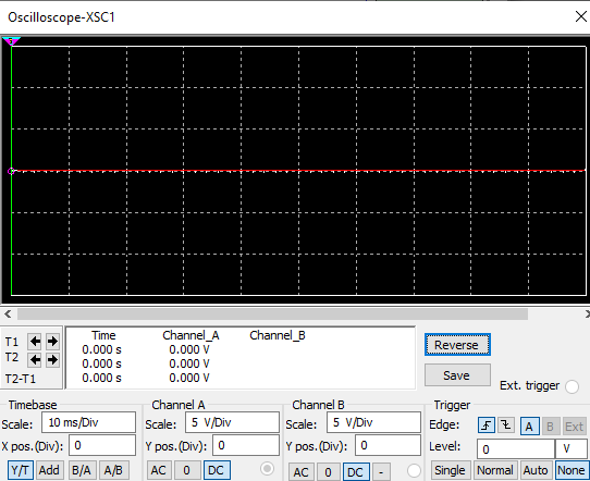
2)When Switch A is Close and B is open(FORWARD Direction)

3) When switch B is close and A is open(REVERSE Direction)

Here i have uploaded ckt diagram and responses.
In responses 2 & 3 at first switches were open. so response in first division is at 0. Then when switch is closed, we can see the curve changing w.r.t. Direction.
If you have any doubt, let me know.
Add Answer to:
can any one help me drow this circuit in multisim and get the
simulation output plz...
Can someone help me derive the general equation for the Acm (when it is a single-ended...
 Can someone help me derive the general equation for the Acm
(when it is a single-ended common-mode gain) for Q1,Q2 and Q4? I
know the general formula for Q1 and Q2 are going to be the same but
Q4 is going to be different because you have to take into account
ro.
In this assignment, you will design a differential amplifier satisfying the required differential gain, input impedance, and single-ended common-mode gain; when fed by a small-signal. Then you will...
Can someone help me derive the general equation for the Acm
(when it is a single-ended common-mode gain) for Q1,Q2 and Q4? I
know the general formula for Q1 and Q2 are going to be the same but
Q4 is going to be different because you have to take into account
ro.
In this assignment, you will design a differential amplifier satisfying the required differential gain, input impedance, and single-ended common-mode gain; when fed by a small-signal. Then you will...
Hi everyone, I have a problem about multistage amplifier. Please help me out, Thank you. Consider...
 Hi everyone, I have a problem about multistage amplifier.
Please help me out, Thank you.
Consider the following multistage amplifier circuit. Given, B VA = 0, VcCE(Sat) = 0.2V and IVBE(ON) 0.7V for all transistors except Q3. VBE for Q3 is 0.655V. Determine the output voltage R6 1.8kΩ R1 9.77ko R2 24k0 R3 4kn R4 10ko R5 10ko 15 V Q8 Q10 Q5 Q6 output Q3 Q2 Q1 R9 15.7k R7 10kn R8 900 15 V
Hi everyone, I have a problem about multistage amplifier.
Please help me out, Thank you.
Consider the following multistage amplifier circuit. Given, B VA = 0, VcCE(Sat) = 0.2V and IVBE(ON) 0.7V for all transistors except Q3. VBE for Q3 is 0.655V. Determine the output voltage R6 1.8kΩ R1 9.77ko R2 24k0 R3 4kn R4 10ko R5 10ko 15 V Q8 Q10 Q5 Q6 output Q3 Q2 Q1 R9 15.7k R7 10kn R8 900 15 V
Q1. The values of the difference amplifier in figure 1 are Ao 5x 10⁵, Rı =...
 Q1. The values of the difference amplifier in figure 1 are Ao 5x 10⁵, Rı = 5kQ, RF = 50M, Ra-2kQ, and Rx-20kS2. The input voltages are vb-5mV and Va--15mV. Find the out voltage vo. (5 Points) RF R1 Figure 1 Q2. Design an integrator as shown in figure 2 to be operated with an AC signal of 5 kHz and to give a closed loop voltage gain of Af-10 at w=1 rad/s. (5 Points) iRF RI 79 +Vcc 2...
1. Can you help me convert this circuit into a small - signal equivalent circuit? 2. Can you tell me how to calculate R...
 1. Can you help me convert this circuit into a small - signal
equivalent circuit?
2. Can you tell me how to calculate Rin and Rout directly in
that circuit?
3. Also I wanna know about values of Rin, Rout, VGD(voltage
between gate-drain), Av(entire voltage gain)
스를 잡도록 하였다. 또한, M3와 R1으로 전류원을 구성하여 능동 부하 M2의 바이어 해서 입력 바이어 스를 잡도록 하였다. FDC6322CP FDC6322CP V1 M3 M2 5Vdc V4 C2 5Vdc R1 30 1u R4 10k R3 10k...
1. Can you help me convert this circuit into a small - signal
equivalent circuit?
2. Can you tell me how to calculate Rin and Rout directly in
that circuit?
3. Also I wanna know about values of Rin, Rout, VGD(voltage
between gate-drain), Av(entire voltage gain)
스를 잡도록 하였다. 또한, M3와 R1으로 전류원을 구성하여 능동 부하 M2의 바이어 해서 입력 바이어 스를 잡도록 하였다. FDC6322CP FDC6322CP V1 M3 M2 5Vdc V4 C2 5Vdc R1 30 1u R4 10k R3 10k...
Homework 4 Due: June 26, 2019, at 5 pm. Note: Show all steps required to get...
 Homework 4 Due: June 26, 2019, at 5 pm. Note: Show all steps required to get to your answers and make sure to box them. Writing down answers to questions asked without any explanation(s) will not do it. Clarity should be a priority Moreover, the assigned textbook for this class is Sedra and Smith, Microelectronic Circuits, Seventh Edition, Oxford University Press. Make sure you have the proper book Reminder: In class, we have expressed the overall voltage gain of a...
Homework 4 Due: June 26, 2019, at 5 pm. Note: Show all steps required to get...
 Homework 4 Due: June 26, 2019, at 5 pm. Note: Show all steps required to get to your answers and make sure to box them. Writing down answers to questions asked without any explanation(s) will not do it. Clarity should be a priority Moreover, the assigned textbook for this class is Sedra and Smith, Microelectronic Circuits, Seventh Edition, Oxford Univers ity Press. Make sure you have the proper book Reminder: In class, we have expressed the overall voltage gain of...
 Can someone help me derive the general equation for the Acm
(when it is a single-ended common-mode gain) for Q1,Q2 and Q4? I
know the general formula for Q1 and Q2 are going to be the same but
Q4 is going to be different because you have to take into account
ro.
In this assignment, you will design a differential amplifier satisfying the required differential gain, input impedance, and single-ended common-mode gain; when fed by a small-signal. Then you will...
Can someone help me derive the general equation for the Acm
(when it is a single-ended common-mode gain) for Q1,Q2 and Q4? I
know the general formula for Q1 and Q2 are going to be the same but
Q4 is going to be different because you have to take into account
ro.
In this assignment, you will design a differential amplifier satisfying the required differential gain, input impedance, and single-ended common-mode gain; when fed by a small-signal. Then you will...
 Hi everyone, I have a problem about multistage amplifier.
Please help me out, Thank you.
Consider the following multistage amplifier circuit. Given, B VA = 0, VcCE(Sat) = 0.2V and IVBE(ON) 0.7V for all transistors except Q3. VBE for Q3 is 0.655V. Determine the output voltage R6 1.8kΩ R1 9.77ko R2 24k0 R3 4kn R4 10ko R5 10ko 15 V Q8 Q10 Q5 Q6 output Q3 Q2 Q1 R9 15.7k R7 10kn R8 900 15 V
Hi everyone, I have a problem about multistage amplifier.
Please help me out, Thank you.
Consider the following multistage amplifier circuit. Given, B VA = 0, VcCE(Sat) = 0.2V and IVBE(ON) 0.7V for all transistors except Q3. VBE for Q3 is 0.655V. Determine the output voltage R6 1.8kΩ R1 9.77ko R2 24k0 R3 4kn R4 10ko R5 10ko 15 V Q8 Q10 Q5 Q6 output Q3 Q2 Q1 R9 15.7k R7 10kn R8 900 15 V
 Q1. The values of the difference amplifier in figure 1 are Ao 5x 10⁵, Rı = 5kQ, RF = 50M, Ra-2kQ, and Rx-20kS2. The input voltages are vb-5mV and Va--15mV. Find the out voltage vo. (5 Points) RF R1 Figure 1 Q2. Design an integrator as shown in figure 2 to be operated with an AC signal of 5 kHz and to give a closed loop voltage gain of Af-10 at w=1 rad/s. (5 Points) iRF RI 79 +Vcc 2...
 1. Can you help me convert this circuit into a small - signal
equivalent circuit?
2. Can you tell me how to calculate Rin and Rout directly in
that circuit?
3. Also I wanna know about values of Rin, Rout, VGD(voltage
between gate-drain), Av(entire voltage gain)
스를 잡도록 하였다. 또한, M3와 R1으로 전류원을 구성하여 능동 부하 M2의 바이어 해서 입력 바이어 스를 잡도록 하였다. FDC6322CP FDC6322CP V1 M3 M2 5Vdc V4 C2 5Vdc R1 30 1u R4 10k R3 10k...
1. Can you help me convert this circuit into a small - signal
equivalent circuit?
2. Can you tell me how to calculate Rin and Rout directly in
that circuit?
3. Also I wanna know about values of Rin, Rout, VGD(voltage
between gate-drain), Av(entire voltage gain)
스를 잡도록 하였다. 또한, M3와 R1으로 전류원을 구성하여 능동 부하 M2의 바이어 해서 입력 바이어 스를 잡도록 하였다. FDC6322CP FDC6322CP V1 M3 M2 5Vdc V4 C2 5Vdc R1 30 1u R4 10k R3 10k...
 Homework 4 Due: June 26, 2019, at 5 pm. Note: Show all steps required to get to your answers and make sure to box them. Writing down answers to questions asked without any explanation(s) will not do it. Clarity should be a priority Moreover, the assigned textbook for this class is Sedra and Smith, Microelectronic Circuits, Seventh Edition, Oxford University Press. Make sure you have the proper book Reminder: In class, we have expressed the overall voltage gain of a...
 Homework 4 Due: June 26, 2019, at 5 pm. Note: Show all steps required to get to your answers and make sure to box them. Writing down answers to questions asked without any explanation(s) will not do it. Clarity should be a priority Moreover, the assigned textbook for this class is Sedra and Smith, Microelectronic Circuits, Seventh Edition, Oxford Univers ity Press. Make sure you have the proper book Reminder: In class, we have expressed the overall voltage gain of...
Most questions answered within 3 hours.
-
Where is the error in this code sequence?
String s1 = "Hello";
String s2 = "ello";...
asked 10 months ago -
Financial data for Joel de Paris, Inc., for last year
follow:
Joel de Paris, Inc.
Balance...
asked 10 months ago -
Consider this reaction:
Al2(SO4)3 (aq)+ BaCl3
(aq) Al2Cl6 (aq)- +
3BaSO4(s) . What is the...
asked 10 months ago -
Suppose that Savneet is considering increasing her
recent random sample from 20 car rentals to 40...
asked 10 months ago -
Trucks arrive at an unloading terminal at an average rate of 120
per hour.
Trucks arrive...
asked 10 months ago -
Why are methanol and ethanol completely soluble in water while
octanol is not very little soluble....
asked 10 months ago -
A facilities manager at a university reads in a research report
that the mean amount of...
asked 10 months ago -
When the CuSO4 is rehydrated by adding water to the anhydrous
compound, is this an endothermic...
asked 10 months ago -
A ray of sunlight is passing from diamond into crown glass; the
angle of incidence is...
asked 10 months ago -
A block of mass 0.249 kg is placed on top of a light, vertical
spring of...
asked 10 months ago -
how do the kidneys compensate in the presences of acidosis
a) trigger hyperventilate
b) reserve acid...
asked 10 months ago -
Question 501 pts
The rental rate of capital to the firm increases. Which of the
following...
asked 10 months ago