

Also explain in words what this means. Assuming that Q2 Q1 and Q0 are LEDs from left to right respectively, and D2, D1, and D0 are switches from left to right respectively. Just explain a few states for my understanding.
Homework Answers
When the present state is Q2 = 0, Q1 = 0, Q0 = 0
The logic circuit is marked with the output and the the output of different gates as below
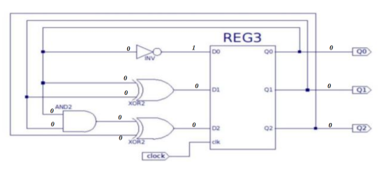
So now, D0 = 1, D1 = 0, D2 =0
So when the clock comes, the output will become Q0 = D0 =1, Q1 = D1 = 0, Q2 = D2 = 0. So the next state is Q2 = 0, Q1 = 0, Q0 = 1. The next state of a D flip flop is the content given to the D pin
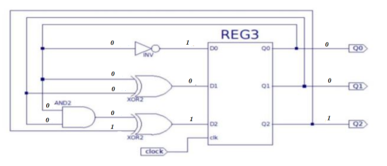
When the present state is Q2 = 0, Q1 = 0, Q0 = 1
The logic circuit is marked with the output and the the output of different gates as below

So now, D0 = 0, D1 = 1, D2 =0
So when the clock comes, the output will become Q0 = D0 =0, Q1 = D1 = 1, Q2 = D2 = 0. So the next state is Q2 = 0, Q1 = 1, Q0 = 0. The next state of a D flip flop is the content given to the D pin
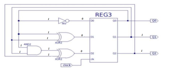
When the present state is Q2 = 0, Q1 = 1, Q0 = 0
The logic circuit is marked with the output and the the output of different gates as below

So now, D0 = 1, D1 = 1, D2 =0
So when the clock comes, the output will become Q0 = D0 =1, Q1 = D1 = 1, Q2 = D2 = 0. So the next state is Q2 = 0, Q1 = 1, Q0 = 1. The next state of a D flip flop is the content given to the D pin
When the present state is Q2 = 0, Q1 = 1, Q0 = 1
The logic circuit is marked with the output and the the output of different gates as below

So now, D0 = 0, D1 = 0, D2 = 1
So when the clock comes, the output will become Q0 = D0 =0, Q1 = D1 = 0, Q2 = D2 = 1. So the next state is Q2 = 1, Q1 = 0, Q0 = 0. The next state of a D flip flop is the content given to the D pin
When the present state is Q2 = 1, Q1 = 0, Q0 = 0
The logic circuit is marked with the output and the the output of different gates as below
So now, D0 = 1, D1 = 0, D2 = 1
So when the clock comes, the output will become Q0 = D0 =1, Q1 = D1 = 0, Q2 = D2 = 1. So the next state is Q2 = 1, Q1 = 0, Q0 = 1. The next state of a D flip flop is the content given to the D pin
When the present state is Q2 = 1, Q1 = 0, Q0 = 1
The logic circuit is marked with the output and the the output of different gates as below

So now, D0 = 0, D1 = 1, D2 = 1
So when the clock comes, the output will become Q0 = D0 =0, Q1 = D1 = 1, Q2 = D2 = 1. So the next state is Q2 = 1, Q1 = 1, Q0 = 0. The next state of a D flip flop is the content given to the D pin
When the present state is Q2 = 1, Q1 = 1, Q0 = 0
The logic circuit is marked with the output and the the output of different gates as below

So now, D0 = 1, D1 = 1, D2 = 1
So when the clock comes, the output will become Q0 = D0 =1, Q1 = D1 = 1, Q2 = D2 = 1. So the next state is Q2 = 1, Q1 = 1, Q0 = 1. The next state of a D flip flop is the content given to the D pin
When the present state is Q2 = 1, Q1 = 1, Q0 = 1
The logic circuit is marked with the output and the the output of different gates as below
So now, D0 = 0, D1 = 0, D2 = 0
So when the clock comes, the output will become Q0 = D0 =0, Q1 = D1 = 0, Q2 = D2 = 0. So the next state is Q2 = 0, Q1 = 0, Q0 = 0. The next state of a D flip flop is the content given to the D pin
So the table can be filled as

Add Answer to:
Also explain in words what this means. Assuming that Q2 Q1 and
Q0 are LEDs from...
The following is an equivalent way of creating the circuit above. Below is the truth table...
 The following is an equivalent way of creating the circuit
above.
Below is the truth table
Q2, Q1, and Q0 are LED outputs from left to right respectively
and D2, D1, and D0 are switches from left to right respectively
Answer the following questions:
1. What signal(s) represent the present state and next state of
the circuit?
2. Sketch a Finite State Machine diagram of the circuit (Be sure
to show inputs and outputs).
3. Describe the high-level behavior of...
The following is an equivalent way of creating the circuit
above.
Below is the truth table
Q2, Q1, and Q0 are LED outputs from left to right respectively
and D2, D1, and D0 are switches from left to right respectively
Answer the following questions:
1. What signal(s) represent the present state and next state of
the circuit?
2. Sketch a Finite State Machine diagram of the circuit (Be sure
to show inputs and outputs).
3. Describe the high-level behavior of...
The following three images accompany one another. The second image is another version of the first...
 The following three images accompany one another. The second
image is another version of the first which we are using in the
example. How does image 4 change the function of the circuit (an
input, 'a', has been added that logically influences the next state
bits)?? Fill out the truth table to show the change.
Note: Q2, Q1, and Q0 are LED outputs from left to right
respectively. D2, D1, and D0 are switches from left to right
respectively. 'a'...
The following three images accompany one another. The second
image is another version of the first which we are using in the
example. How does image 4 change the function of the circuit (an
input, 'a', has been added that logically influences the next state
bits)?? Fill out the truth table to show the change.
Note: Q2, Q1, and Q0 are LED outputs from left to right
respectively. D2, D1, and D0 are switches from left to right
respectively. 'a'...
What is the function of this circuit? It is a sequential circuit with no external inputs....
 What is the function of this circuit? It is a sequential circuit
with no external inputs. Draw a schematic using the Flip-Flop
diagram below that performs the task it is intended to. The design
will eventually be programmed to an FPGA board.
REG3 DO 00 QO DI 01 101 XORZ AND2 02 02 Q2 XOR2 cik clock D[2] D[1] D[O] D Flip-Flop Flip-Flop Flip-Flop sw_in en sw_in sw_in clock clock clock Q[2] Q[1] Q[o]
What is the function of this circuit? It is a sequential circuit
with no external inputs. Draw a schematic using the Flip-Flop
diagram below that performs the task it is intended to. The design
will eventually be programmed to an FPGA board.
REG3 DO 00 QO DI 01 101 XORZ AND2 02 02 Q2 XOR2 cik clock D[2] D[1] D[O] D Flip-Flop Flip-Flop Flip-Flop sw_in en sw_in sw_in clock clock clock Q[2] Q[1] Q[o]
Design a 3- bit Multipurpose Register. The register utilizes 3 "D" type flip flops with outputs...
Design a 3- bit Multipurpose Register. The register utilizes 3 "D" type flip flops with outputs Q0, Q1, Q2. The Registers has a synchronous clock input(CLK) that clocks all 3 flip flops on its positive edge The Registers has an asynchronous clear input(CLR' ) that sets all flip flops to "0" when active low. The Register has 2 select inputs, S0 and S1 that selects the functions as folows: S1 = 0, 0, 1, 1 and S0 = 0,1,0,1 and...
Problem 7. Consider the 74x194 4-bit bidirectional universal shift register shown below Determine the operation of...
 Problem 7. Consider the 74x194 4-bit bidirectional universal shift register shown below Determine the operation of this circuit by filling out the table. Assume that the register is cleared initially as indicated by the first row in the table, and then connected to +5V (before time t), as shown in schematic. Also assume that t 'is that time at which a positive edge occurs in the input signal 'clock'. Si and S0 inputs (given) are used to switch between modes...
Please help Q15. A watch can display one of four items: Time, Alarm, Stopwatch or Date, controlled by two signals Q1 and Q0 (00 time, 01 alarm, 10 stopwatch, 11date). Assume Q1 and Q0 control an N...
 Please help
Q15. A watch can display one of four items: Time, Alarm, Stopwatch or Date, controlled by two signals Q1 and Q0 (00 time, 01 alarm, 10 stopwatch, 11date). Assume Q1 and Q0 control an N-bit MUX that passes the correct register to the display. Pressing a button B (sets B-1) sequences the display to the next item, releasing the button resets B-0 and the display remains stable. For example, if the current displayed item is the date the...
Please help
Q15. A watch can display one of four items: Time, Alarm, Stopwatch or Date, controlled by two signals Q1 and Q0 (00 time, 01 alarm, 10 stopwatch, 11date). Assume Q1 and Q0 control an N-bit MUX that passes the correct register to the display. Pressing a button B (sets B-1) sequences the display to the next item, releasing the button resets B-0 and the display remains stable. For example, if the current displayed item is the date the...
The task is to design a two-bit controlled counter which has two counting bits (Q2, Q1), has one control input C1, and a...
 The task is to design a two-bit controlled counter which has two
counting bits (Q2, Q1), has one control input C1, and also two
extra outputs, one indicating overflow, the other underflow.
When C1=0 the counter counts up by 2s; i.e. 0 becomes 2, 1
becomes 3. In this mode the values 2 and 3 go to the overflow
state. When the control input C1=1, the counter counts down by 2s,
i.e. 3 becomes 1, and 2 becomes 0, and...
The task is to design a two-bit controlled counter which has two
counting bits (Q2, Q1), has one control input C1, and also two
extra outputs, one indicating overflow, the other underflow.
When C1=0 the counter counts up by 2s; i.e. 0 becomes 2, 1
becomes 3. In this mode the values 2 and 3 go to the overflow
state. When the control input C1=1, the counter counts down by 2s,
i.e. 3 becomes 1, and 2 becomes 0, and...
Design a counter to count-up from 2 to 5 using 3 D Flip-Flops similar to the...
 Design a counter to count-up from 2 to 5 using 3 D Flip-Flops similar to the following sample: Important Steps: After you simplify D2, D1 and DO by kmap Have a piece of paper to draw it then open iCircuit to design it using BCD If it works well as a counter, copy the design from iCircuit and paste it here. 3-Bit Counter Using D Flip-Flop: The State Equation of D Flip-Flop: Q(t+1)=D(t) => Dn=An Count Up From 3 To...
I am making a 4-bit universal shift register that can perform right shift, left shift, and...
 I am making a 4-bit universal shift register that can perform
right shift, left shift, and parallel loading using 4-to-1
multiplexers in VHDL. I keep getting red lines for u3, u2, u1, u0.
The error says the following below. What is wrong with my code? How
can I fix it?
librarviees, use ieee.std_logic_1164.all; entity uni shift.reg.is porti 1 : in std. Jogis vector (3 downto.0); I, w, clock : in std logici 9: buffer std. Jogis vector (3 downto 0));...
I am making a 4-bit universal shift register that can perform
right shift, left shift, and parallel loading using 4-to-1
multiplexers in VHDL. I keep getting red lines for u3, u2, u1, u0.
The error says the following below. What is wrong with my code? How
can I fix it?
librarviees, use ieee.std_logic_1164.all; entity uni shift.reg.is porti 1 : in std. Jogis vector (3 downto.0); I, w, clock : in std logici 9: buffer std. Jogis vector (3 downto 0));...
Basically it is asking to draw the state machine using the D-flipflops and the ICs provided....
 Basically it is asking to draw the state machine using the
D-flipflops and the ICs provided.
6.1.4 Simulation Draw the the elevator controller. You must use the ICs listed for this laboratory, i.e., you will need bubble-to-bubble logic to implement the OR functions. Connect the CLK inputs of the flip-flops to a CLOCK signal, and the asynchronous CLR inputs to an active low RESET signal. 25 The sequence of commands to be applied for simulating the elevator controller is (starting...
Basically it is asking to draw the state machine using the
D-flipflops and the ICs provided.
6.1.4 Simulation Draw the the elevator controller. You must use the ICs listed for this laboratory, i.e., you will need bubble-to-bubble logic to implement the OR functions. Connect the CLK inputs of the flip-flops to a CLOCK signal, and the asynchronous CLR inputs to an active low RESET signal. 25 The sequence of commands to be applied for simulating the elevator controller is (starting...
 The following is an equivalent way of creating the circuit
above.
Below is the truth table
Q2, Q1, and Q0 are LED outputs from left to right respectively
and D2, D1, and D0 are switches from left to right respectively
Answer the following questions:
1. What signal(s) represent the present state and next state of
the circuit?
2. Sketch a Finite State Machine diagram of the circuit (Be sure
to show inputs and outputs).
3. Describe the high-level behavior of...
The following is an equivalent way of creating the circuit
above.
Below is the truth table
Q2, Q1, and Q0 are LED outputs from left to right respectively
and D2, D1, and D0 are switches from left to right respectively
Answer the following questions:
1. What signal(s) represent the present state and next state of
the circuit?
2. Sketch a Finite State Machine diagram of the circuit (Be sure
to show inputs and outputs).
3. Describe the high-level behavior of...
 The following three images accompany one another. The second
image is another version of the first which we are using in the
example. How does image 4 change the function of the circuit (an
input, 'a', has been added that logically influences the next state
bits)?? Fill out the truth table to show the change.
Note: Q2, Q1, and Q0 are LED outputs from left to right
respectively. D2, D1, and D0 are switches from left to right
respectively. 'a'...
The following three images accompany one another. The second
image is another version of the first which we are using in the
example. How does image 4 change the function of the circuit (an
input, 'a', has been added that logically influences the next state
bits)?? Fill out the truth table to show the change.
Note: Q2, Q1, and Q0 are LED outputs from left to right
respectively. D2, D1, and D0 are switches from left to right
respectively. 'a'...
 What is the function of this circuit? It is a sequential circuit
with no external inputs. Draw a schematic using the Flip-Flop
diagram below that performs the task it is intended to. The design
will eventually be programmed to an FPGA board.
REG3 DO 00 QO DI 01 101 XORZ AND2 02 02 Q2 XOR2 cik clock D[2] D[1] D[O] D Flip-Flop Flip-Flop Flip-Flop sw_in en sw_in sw_in clock clock clock Q[2] Q[1] Q[o]
What is the function of this circuit? It is a sequential circuit
with no external inputs. Draw a schematic using the Flip-Flop
diagram below that performs the task it is intended to. The design
will eventually be programmed to an FPGA board.
REG3 DO 00 QO DI 01 101 XORZ AND2 02 02 Q2 XOR2 cik clock D[2] D[1] D[O] D Flip-Flop Flip-Flop Flip-Flop sw_in en sw_in sw_in clock clock clock Q[2] Q[1] Q[o]
 Problem 7. Consider the 74x194 4-bit bidirectional universal shift register shown below Determine the operation of this circuit by filling out the table. Assume that the register is cleared initially as indicated by the first row in the table, and then connected to +5V (before time t), as shown in schematic. Also assume that t 'is that time at which a positive edge occurs in the input signal 'clock'. Si and S0 inputs (given) are used to switch between modes...
 Please help
Q15. A watch can display one of four items: Time, Alarm, Stopwatch or Date, controlled by two signals Q1 and Q0 (00 time, 01 alarm, 10 stopwatch, 11date). Assume Q1 and Q0 control an N-bit MUX that passes the correct register to the display. Pressing a button B (sets B-1) sequences the display to the next item, releasing the button resets B-0 and the display remains stable. For example, if the current displayed item is the date the...
Please help
Q15. A watch can display one of four items: Time, Alarm, Stopwatch or Date, controlled by two signals Q1 and Q0 (00 time, 01 alarm, 10 stopwatch, 11date). Assume Q1 and Q0 control an N-bit MUX that passes the correct register to the display. Pressing a button B (sets B-1) sequences the display to the next item, releasing the button resets B-0 and the display remains stable. For example, if the current displayed item is the date the...
 The task is to design a two-bit controlled counter which has two
counting bits (Q2, Q1), has one control input C1, and also two
extra outputs, one indicating overflow, the other underflow.
When C1=0 the counter counts up by 2s; i.e. 0 becomes 2, 1
becomes 3. In this mode the values 2 and 3 go to the overflow
state. When the control input C1=1, the counter counts down by 2s,
i.e. 3 becomes 1, and 2 becomes 0, and...
The task is to design a two-bit controlled counter which has two
counting bits (Q2, Q1), has one control input C1, and also two
extra outputs, one indicating overflow, the other underflow.
When C1=0 the counter counts up by 2s; i.e. 0 becomes 2, 1
becomes 3. In this mode the values 2 and 3 go to the overflow
state. When the control input C1=1, the counter counts down by 2s,
i.e. 3 becomes 1, and 2 becomes 0, and...
 Design a counter to count-up from 2 to 5 using 3 D Flip-Flops similar to the following sample: Important Steps: After you simplify D2, D1 and DO by kmap Have a piece of paper to draw it then open iCircuit to design it using BCD If it works well as a counter, copy the design from iCircuit and paste it here. 3-Bit Counter Using D Flip-Flop: The State Equation of D Flip-Flop: Q(t+1)=D(t) => Dn=An Count Up From 3 To...
 I am making a 4-bit universal shift register that can perform
right shift, left shift, and parallel loading using 4-to-1
multiplexers in VHDL. I keep getting red lines for u3, u2, u1, u0.
The error says the following below. What is wrong with my code? How
can I fix it?
librarviees, use ieee.std_logic_1164.all; entity uni shift.reg.is porti 1 : in std. Jogis vector (3 downto.0); I, w, clock : in std logici 9: buffer std. Jogis vector (3 downto 0));...
I am making a 4-bit universal shift register that can perform
right shift, left shift, and parallel loading using 4-to-1
multiplexers in VHDL. I keep getting red lines for u3, u2, u1, u0.
The error says the following below. What is wrong with my code? How
can I fix it?
librarviees, use ieee.std_logic_1164.all; entity uni shift.reg.is porti 1 : in std. Jogis vector (3 downto.0); I, w, clock : in std logici 9: buffer std. Jogis vector (3 downto 0));...
 Basically it is asking to draw the state machine using the
D-flipflops and the ICs provided.
6.1.4 Simulation Draw the the elevator controller. You must use the ICs listed for this laboratory, i.e., you will need bubble-to-bubble logic to implement the OR functions. Connect the CLK inputs of the flip-flops to a CLOCK signal, and the asynchronous CLR inputs to an active low RESET signal. 25 The sequence of commands to be applied for simulating the elevator controller is (starting...
Basically it is asking to draw the state machine using the
D-flipflops and the ICs provided.
6.1.4 Simulation Draw the the elevator controller. You must use the ICs listed for this laboratory, i.e., you will need bubble-to-bubble logic to implement the OR functions. Connect the CLK inputs of the flip-flops to a CLOCK signal, and the asynchronous CLR inputs to an active low RESET signal. 25 The sequence of commands to be applied for simulating the elevator controller is (starting...
Most questions answered within 3 hours.
-
Where is the error in this code sequence?
String s1 = "Hello";
String s2 = "ello";...
asked 10 months ago -
Financial data for Joel de Paris, Inc., for last year
follow:
Joel de Paris, Inc.
Balance...
asked 10 months ago -
Consider this reaction:
Al2(SO4)3 (aq)+ BaCl3
(aq) Al2Cl6 (aq)- +
3BaSO4(s) . What is the...
asked 10 months ago -
Suppose that Savneet is considering increasing her
recent random sample from 20 car rentals to 40...
asked 10 months ago -
Trucks arrive at an unloading terminal at an average rate of 120
per hour.
Trucks arrive...
asked 10 months ago -
Why are methanol and ethanol completely soluble in water while
octanol is not very little soluble....
asked 10 months ago -
A facilities manager at a university reads in a research report
that the mean amount of...
asked 10 months ago -
When the CuSO4 is rehydrated by adding water to the anhydrous
compound, is this an endothermic...
asked 10 months ago -
A ray of sunlight is passing from diamond into crown glass; the
angle of incidence is...
asked 10 months ago -
A block of mass 0.249 kg is placed on top of a light, vertical
spring of...
asked 10 months ago -
how do the kidneys compensate in the presences of acidosis
a) trigger hyperventilate
b) reserve acid...
asked 10 months ago -
Question 501 pts
The rental rate of capital to the firm increases. Which of the
following...
asked 10 months ago