
Homework Answers
Add Answer to:
8.3 Consider a conventional NPN BJT with uniform doping. The base-emitter junction is forward biased, and...
3. A silicon npn bipolar transistor is uniformly doped and biased in the forward active region wi...
 3. A silicon npn bipolar transistor is uniformly doped and biased in the forward active region with the base-collector junction reverse biased by 2.5 V. The metallurgical base width is 1.5 μm. The emitter, base collector doping concentrations are 5 × 10¹⁷, 1016, 2 × 1015 cm-3 respectively. a. At T-300 K, calculate the base-emitter voltage at which the minority carrier electron concentration at x-0 is 20% of the majority carrier hole concentration. At this voltage calculate the minority carrier...
Consider a silicon device (which happens to be an npn bipolar transistor) with an emitter doping...
Consider a silicon device (which happens to be an npn bipolar transistor) with an emitter doping of 10^17/cm3, a base doping of 8x10^15/cm3 and a collector doping of 2x10^15/cm3. Carefully calculate how the band diagram, charge density, electric field and electrostatic potential as a function of distance for this device changes from the equilibrium case when this bipolar transistor is properly biased to work as an amplifier. In other words, show how the band diagram changes when the emitter-base junction...
A uniformly doped silicon pnp transistor with base width of 2um is biased in forward active mode (with BC junction reverse biased). The doping concentrations are NE-1018cm NB-5x1016cm3, and Nc-1015cm...
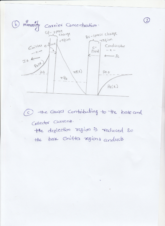
 A uniformly doped silicon pnp transistor with base width of 2um is biased in forward active mode (with BC junction reverse biased). The doping concentrations are NE-1018cm NB-5x1016cm3, and Nc-1015cm3. Assume DB-25 cm2/s, TB-10-s and LB 16um (a) Calculate the values of no, рво, and nco. (b) For VEB 0.65V, determine the respective minority carrier concentration at the edge of the depletion layer, pa(0) and ne(0) (c) Sketch the minority carrier concentration through the device and label each curve (d)...
Forward Active Reverse Active Cutoff Saturation 2. The minority carrier distribution in a NPN BJT under forward acti...
 Forward Active Reverse Active Cutoff Saturation 2. The minority carrier distribution in a NPN BJT under forward active bias is given in the following questions. On top of the figure, sketch the corresponding new minority carrier concentration when the given condition is changed. (To make the question simple, you may assume the depletion width remains unchanged in all questions. But you have to indicate the new equilibrium minority concentration if they are affected.) 6. a) collector doping is increased by...
Problem 2. A silicon NPN bipolar transistor has the following specifications: Emitter: N+: ND =1018 cm-3...
Problem 2. A silicon NPN bipolar transistor has the following specifications: Emitter: N+: ND =1018 cm-3 , base: p-type, NA=1015 cm-3, collector: N-type, ND=5x1015 cm-3 . 1. Draw the energy band diagram of the transistor at thermal equilibrium, 2. If the transistor is biased at Normal Active Mode, emitter-base junction forward biased with 1 V, and collector-base junction is reverse biased with 4V, draw the energy band diagram.
The electron and hole currents inside a pnp BJT biased in the active mode are plotted below. All the currents are referenced to Ii, the hole current inj c cted Determine: (a) The emitter efficiency (...
 The electron and hole currents inside a pnp BJT biased in the active mode are plotted below. All the currents are referenced to Ii, the hole current inj c cted Determine: (a) The emitter efficiency (); (b) The base transport factor (a) (c) The common emitter d.c. current gain (Bac); (d) The base current (IB). (e) For the given transistor, is the recombination-generation current arising from the depletion regions negligible as assumed in the ideal transistor analysis? Explain. Hole current...
Emitter Base Collector 5. Figure illustrates the minority carrier concentrations along a BJT. We are told...
 Emitter Base Collector 5. Figure illustrates the minority carrier concentrations along a BJT. We are told that VEB>0 and VcB>0 according to polarity shown in the figure. State the type of the transistor and the mode in which it is operating a. PNP, active mode b. NPN, saturation mode c. NPN, reverse active mode d. PNP, cut-off mode +V
2. (15 pts) An npn bipolar junction transistor is biased in the forward-active region. The common-base...
 2. (15 pts) An npn bipolar junction transistor is biased in the forward-active region. The common-base current gain, α 0.95. The input emitter current is IE-4.6 mA. a) Calculate the collector current Ic b) Calculate the common-emitter current gain, B c) Calculate the base current IB IB
Consider the npn BJT with a turn-on voltage V1 = 0.70 V, and a saturation emitter-collector...
 Consider the npn BJT with a turn-on voltage V1 = 0.70 V, and a saturation emitter-collector voltage V CE/SAT) = 0.20 V. (a) [20 points) Consider this transistor in a common- emitter circuit (Re = 0). Design this common- emitter circuit to produce the IV (Ic vs. VCE) characteristic and load line (LL) as shown in the graph. Your answers are the following: a drawing of the circuit; the values of Vcc, Rc, VBB, and Ra; and the value for...
P2. Assume that the BJT (of P1) operates in the active mode and the applied voltages...
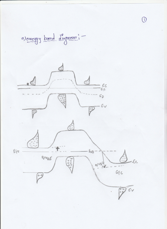
 P2. Assume that the BJT (of P1) operates in the active mode and the applied voltages are: V 0.5V and V-2V. The Shockley assumptions apply (Uniform doping in the individual doping regions, abrupt junctions, low-level injection, no losses due to generation and recombination in the depletion regions). a) Schematically sketch the energy band diagram in the active mode. Indicate the quasi Fermi levels and the width of the space charge regions. b) The voltage Vis further increased. As a consequence...
 3. A silicon npn bipolar transistor is uniformly doped and biased in the forward active region with the base-collector junction reverse biased by 2.5 V. The metallurgical base width is 1.5 μm. The emitter, base collector doping concentrations are 5 × 10¹⁷, 1016, 2 × 1015 cm-3 respectively. a. At T-300 K, calculate the base-emitter voltage at which the minority carrier electron concentration at x-0 is 20% of the majority carrier hole concentration. At this voltage calculate the minority carrier...
 A uniformly doped silicon pnp transistor with base width of 2um is biased in forward active mode (with BC junction reverse biased). The doping concentrations are NE-1018cm NB-5x1016cm3, and Nc-1015cm3. Assume DB-25 cm2/s, TB-10-s and LB 16um (a) Calculate the values of no, рво, and nco. (b) For VEB 0.65V, determine the respective minority carrier concentration at the edge of the depletion layer, pa(0) and ne(0) (c) Sketch the minority carrier concentration through the device and label each curve (d)...
 Forward Active Reverse Active Cutoff Saturation 2. The minority carrier distribution in a NPN BJT under forward active bias is given in the following questions. On top of the figure, sketch the corresponding new minority carrier concentration when the given condition is changed. (To make the question simple, you may assume the depletion width remains unchanged in all questions. But you have to indicate the new equilibrium minority concentration if they are affected.) 6. a) collector doping is increased by...
 The electron and hole currents inside a pnp BJT biased in the active mode are plotted below. All the currents are referenced to Ii, the hole current inj c cted Determine: (a) The emitter efficiency (); (b) The base transport factor (a) (c) The common emitter d.c. current gain (Bac); (d) The base current (IB). (e) For the given transistor, is the recombination-generation current arising from the depletion regions negligible as assumed in the ideal transistor analysis? Explain. Hole current...
 Emitter Base Collector 5. Figure illustrates the minority carrier concentrations along a BJT. We are told that VEB>0 and VcB>0 according to polarity shown in the figure. State the type of the transistor and the mode in which it is operating a. PNP, active mode b. NPN, saturation mode c. NPN, reverse active mode d. PNP, cut-off mode +V
 2. (15 pts) An npn bipolar junction transistor is biased in the forward-active region. The common-base current gain, α 0.95. The input emitter current is IE-4.6 mA. a) Calculate the collector current Ic b) Calculate the common-emitter current gain, B c) Calculate the base current IB IB
 Consider the npn BJT with a turn-on voltage V1 = 0.70 V, and a saturation emitter-collector voltage V CE/SAT) = 0.20 V. (a) [20 points) Consider this transistor in a common- emitter circuit (Re = 0). Design this common- emitter circuit to produce the IV (Ic vs. VCE) characteristic and load line (LL) as shown in the graph. Your answers are the following: a drawing of the circuit; the values of Vcc, Rc, VBB, and Ra; and the value for...
 P2. Assume that the BJT (of P1) operates in the active mode and the applied voltages are: V 0.5V and V-2V. The Shockley assumptions apply (Uniform doping in the individual doping regions, abrupt junctions, low-level injection, no losses due to generation and recombination in the depletion regions). a) Schematically sketch the energy band diagram in the active mode. Indicate the quasi Fermi levels and the width of the space charge regions. b) The voltage Vis further increased. As a consequence...
Most questions answered within 3 hours.
-
Where is the error in this code sequence?
String s1 = "Hello";
String s2 = "ello";...
asked 10 months ago -
Financial data for Joel de Paris, Inc., for last year
follow:
Joel de Paris, Inc.
Balance...
asked 10 months ago -
Consider this reaction:
Al2(SO4)3 (aq)+ BaCl3
(aq) Al2Cl6 (aq)- +
3BaSO4(s) . What is the...
asked 10 months ago -
Suppose that Savneet is considering increasing her
recent random sample from 20 car rentals to 40...
asked 10 months ago -
Trucks arrive at an unloading terminal at an average rate of 120
per hour.
Trucks arrive...
asked 10 months ago -
Why are methanol and ethanol completely soluble in water while
octanol is not very little soluble....
asked 10 months ago -
A facilities manager at a university reads in a research report
that the mean amount of...
asked 10 months ago -
When the CuSO4 is rehydrated by adding water to the anhydrous
compound, is this an endothermic...
asked 10 months ago -
A ray of sunlight is passing from diamond into crown glass; the
angle of incidence is...
asked 10 months ago -
A block of mass 0.249 kg is placed on top of a light, vertical
spring of...
asked 10 months ago -
how do the kidneys compensate in the presences of acidosis
a) trigger hyperventilate
b) reserve acid...
asked 10 months ago -
Question 501 pts
The rental rate of capital to the firm increases. Which of the
following...
asked 10 months ago