
Homework Answers

Add Answer to:
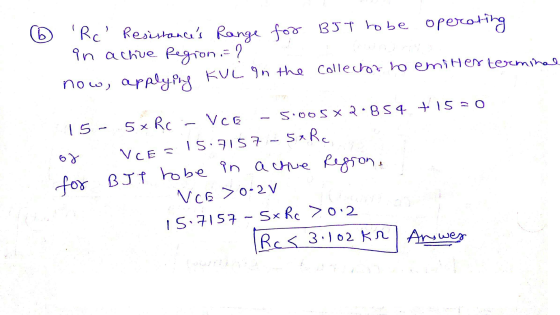
Question #3 (14 points) Assume: B = 100 when active VBE = 0.7V when the base-emitter...
DC Biasing For the circuit below, assume 150, VBE(ON) -0.7V and Vce(SAT)- 0.2V Voc 10 VO...
 DC Biasing For the circuit below, assume 150, VBE(ON) -0.7V and Vce(SAT)- 0.2V Voc 10 VO Rc 3.3K ib Rb 330K Write an equation for ib in terms of Vin (Hint: use KVL from VBB to ground) Write the general equation for ic in terms of ib and P Write an equation for Vce in terms of ic CE- Fill the table Operational Region 0 V 3 V 5 V 7 V
RE -3.3k2 Figure 5. Vbe-0.7V (active), Vce 0.2V (saturation), p-100 For the circuit shown in Figure...
 RE -3.3k2 Figure 5. Vbe-0.7V (active), Vce 0.2V (saturation), p-100 For the circuit shown in Figure 5: a) If V oV DC, find the DC bias point for Q1? b) Draw the small signal equivalent circuit and evaluate the small signal AC voltage gain. c) Sketch le vs Vce and show the operating point for the transistor. d) How would you change the bias to obtain maximum signal swing?
I keep getting the wrong answer from everyone else pls help me get the right answer For the BJT bias circuit shown, what value of Rc in kilohms is needed to allow the maximum possible peak-to-peak si...
 I keep getting the wrong answer from everyone else pls help me
get the right answer
For the BJT bias circuit shown, what value of Rc in kilohms is needed to allow the maximum possible peak-to-peak signal swing on the collector without clipping? Use Vcc-9V, Vee--7V, Vb-1.2V, and Re -9.9k2. Assume that to keep the transistor in the forward-active region, the base-collector junction cannot be forward biased. Use B 20 and Vbe(on) 0.7V. Neglect the effects of base-width modulation. Vcc...
I keep getting the wrong answer from everyone else pls help me
get the right answer
For the BJT bias circuit shown, what value of Rc in kilohms is needed to allow the maximum possible peak-to-peak signal swing on the collector without clipping? Use Vcc-9V, Vee--7V, Vb-1.2V, and Re -9.9k2. Assume that to keep the transistor in the forward-active region, the base-collector junction cannot be forward biased. Use B 20 and Vbe(on) 0.7V. Neglect the effects of base-width modulation. Vcc...
4.3V (15 pts) For the circuit shown, Rc = 2 kQ. Assume that VBE-0.7V, and that...
 4.3V (15 pts) For the circuit shown, Rc = 2 kQ. Assume that VBE-0.7V, and that β very large, resulting in the emitter and collector currents being about equal. a) Determine the value of RE that would result in VcE 3V b) Determine the value of the collector current. c) Determine the value of β, if the base current IB-2μΑ. RE -5.7V
I keep getting the wrong answer from everyone else pls help me get the right answer...
 I keep getting the wrong answer from everyone else pls help me
get the right answer
For the BJT bias circuit shown, what value of Rc in kilohms is needed to allow the maximum possible peak-to-peak signal swing on the collector without clipping? Use Vcc-9V, Vee--7V, Vb-1.2V, and Re -9.9k2. Assume that to keep the transistor in the forward-active region, the base-collector junction cannot be forward biased. Use B 20 and Vbe(on) 0.7V. Neglect the effects of base-width modulation. Vcc...
I keep getting the wrong answer from everyone else pls help me
get the right answer
For the BJT bias circuit shown, what value of Rc in kilohms is needed to allow the maximum possible peak-to-peak signal swing on the collector without clipping? Use Vcc-9V, Vee--7V, Vb-1.2V, and Re -9.9k2. Assume that to keep the transistor in the forward-active region, the base-collector junction cannot be forward biased. Use B 20 and Vbe(on) 0.7V. Neglect the effects of base-width modulation. Vcc...
Consider the npn BJT with a turn-on voltage V1 = 0.70 V, and a saturation emitter-collector...
 Consider the npn BJT with a turn-on voltage V1 = 0.70 V, and a saturation emitter-collector voltage V CE/SAT) = 0.20 V. (a) [20 points) Consider this transistor in a common- emitter circuit (Re = 0). Design this common- emitter circuit to produce the IV (Ic vs. VCE) characteristic and load line (LL) as shown in the graph. Your answers are the following: a drawing of the circuit; the values of Vcc, Rc, VBB, and Ra; and the value for...
It Kind of goes without saying but if you have no knowledge than dont comment or try and answer this question you dope Questions 1-3 below are about the amplifier circuit of Figure 1. Here Vcc is a...
 It
Kind of goes without saying but if you have no knowledge than dont
comment or try and answer this question you dope
Questions 1-3 below are about the amplifier circuit of Figure 1. Here Vcc is a fixed voltage The base voltage vB(t) is time-varying, and is of the form vB(t) V(t) where VB is a DC offset, and vb(t) is a time-varying purely AC signal. Suppose the amplitude of vb is A. Assume that the capacitor C is...
It
Kind of goes without saying but if you have no knowledge than dont
comment or try and answer this question you dope
Questions 1-3 below are about the amplifier circuit of Figure 1. Here Vcc is a fixed voltage The base voltage vB(t) is time-varying, and is of the form vB(t) V(t) where VB is a DC offset, and vb(t) is a time-varying purely AC signal. Suppose the amplitude of vb is A. Assume that the capacitor C is...
For the BJT bias circuit shown, what value of Rc in kilohms is needed to allow...
 For the BJT bias circuit shown, what value of Rc in kilohms is needed to allow the maximum possible peak-to-peak signal swing on the collector without clipping? Use Vcc = 8V, Vee = -6V, Vb = 2.0v, and Re = 9.1k02. Assume that to keep the transistor in the forward-active region, the base- collector junction cannot be forward biased. Use B = 65 and Vbelon) = 0.7V. Neglect the effects of base-width modulation. VCC 芒Vs windows
A Si p-n-p transistor has impurity concentrations of6*1018, 7 1015 and 9*1017 cm3 in the emitter, base and collector regions correspondingly. The corresponding carrier lifetimes are 10 10-7, and...
 A Si p-n-p transistor has impurity concentrations of6*1018, 7 1015 and 9*1017 cm3 in the emitter, base and collector regions correspondingly. The corresponding carrier lifetimes are 10 10-7, and 106 s. The device cross-section area A-0.02 mm2, the emitter base junction is forward biased to 0.7V. Use diffusion coefficients DE-3cm2/s, DB-15 cm2/s, Dc-5cm%, and base with w=0.65 (a) Calculate emitter current using iEp.n-qADpPn p exp( )1 (b) Calculate current gain: (c) Estimate the device switching time (RC) assuming that resistance...
The transistor in the circuit below has ?-100 and Vci(sat) OV. You may use the constant...
 The transistor in the circuit below has ?-100 and Vci(sat) OV. You may use the constant voltage model with VE 0.7V if the base emitter junction is forward biased. A variable DC source is attached to input VIN. Find the operating mode (cutoff, active, or saturation), the collector node voltage VC, and the collector current IC for each of the following cases: (a) VIN 0V (b) VIN = 1.2V (c) VIN 6.0v (d) VIN 12.0V 1 K IC VC 10K...
 DC Biasing For the circuit below, assume 150, VBE(ON) -0.7V and Vce(SAT)- 0.2V Voc 10 VO Rc 3.3K ib Rb 330K Write an equation for ib in terms of Vin (Hint: use KVL from VBB to ground) Write the general equation for ic in terms of ib and P Write an equation for Vce in terms of ic CE- Fill the table Operational Region 0 V 3 V 5 V 7 V
 RE -3.3k2 Figure 5. Vbe-0.7V (active), Vce 0.2V (saturation), p-100 For the circuit shown in Figure 5: a) If V oV DC, find the DC bias point for Q1? b) Draw the small signal equivalent circuit and evaluate the small signal AC voltage gain. c) Sketch le vs Vce and show the operating point for the transistor. d) How would you change the bias to obtain maximum signal swing?
 I keep getting the wrong answer from everyone else pls help me
get the right answer
For the BJT bias circuit shown, what value of Rc in kilohms is needed to allow the maximum possible peak-to-peak signal swing on the collector without clipping? Use Vcc-9V, Vee--7V, Vb-1.2V, and Re -9.9k2. Assume that to keep the transistor in the forward-active region, the base-collector junction cannot be forward biased. Use B 20 and Vbe(on) 0.7V. Neglect the effects of base-width modulation. Vcc...
I keep getting the wrong answer from everyone else pls help me
get the right answer
For the BJT bias circuit shown, what value of Rc in kilohms is needed to allow the maximum possible peak-to-peak signal swing on the collector without clipping? Use Vcc-9V, Vee--7V, Vb-1.2V, and Re -9.9k2. Assume that to keep the transistor in the forward-active region, the base-collector junction cannot be forward biased. Use B 20 and Vbe(on) 0.7V. Neglect the effects of base-width modulation. Vcc...
 4.3V (15 pts) For the circuit shown, Rc = 2 kQ. Assume that VBE-0.7V, and that β very large, resulting in the emitter and collector currents being about equal. a) Determine the value of RE that would result in VcE 3V b) Determine the value of the collector current. c) Determine the value of β, if the base current IB-2μΑ. RE -5.7V
 I keep getting the wrong answer from everyone else pls help me
get the right answer
For the BJT bias circuit shown, what value of Rc in kilohms is needed to allow the maximum possible peak-to-peak signal swing on the collector without clipping? Use Vcc-9V, Vee--7V, Vb-1.2V, and Re -9.9k2. Assume that to keep the transistor in the forward-active region, the base-collector junction cannot be forward biased. Use B 20 and Vbe(on) 0.7V. Neglect the effects of base-width modulation. Vcc...
I keep getting the wrong answer from everyone else pls help me
get the right answer
For the BJT bias circuit shown, what value of Rc in kilohms is needed to allow the maximum possible peak-to-peak signal swing on the collector without clipping? Use Vcc-9V, Vee--7V, Vb-1.2V, and Re -9.9k2. Assume that to keep the transistor in the forward-active region, the base-collector junction cannot be forward biased. Use B 20 and Vbe(on) 0.7V. Neglect the effects of base-width modulation. Vcc...
 Consider the npn BJT with a turn-on voltage V1 = 0.70 V, and a saturation emitter-collector voltage V CE/SAT) = 0.20 V. (a) [20 points) Consider this transistor in a common- emitter circuit (Re = 0). Design this common- emitter circuit to produce the IV (Ic vs. VCE) characteristic and load line (LL) as shown in the graph. Your answers are the following: a drawing of the circuit; the values of Vcc, Rc, VBB, and Ra; and the value for...
 It
Kind of goes without saying but if you have no knowledge than dont
comment or try and answer this question you dope
Questions 1-3 below are about the amplifier circuit of Figure 1. Here Vcc is a fixed voltage The base voltage vB(t) is time-varying, and is of the form vB(t) V(t) where VB is a DC offset, and vb(t) is a time-varying purely AC signal. Suppose the amplitude of vb is A. Assume that the capacitor C is...
It
Kind of goes without saying but if you have no knowledge than dont
comment or try and answer this question you dope
Questions 1-3 below are about the amplifier circuit of Figure 1. Here Vcc is a fixed voltage The base voltage vB(t) is time-varying, and is of the form vB(t) V(t) where VB is a DC offset, and vb(t) is a time-varying purely AC signal. Suppose the amplitude of vb is A. Assume that the capacitor C is...
 For the BJT bias circuit shown, what value of Rc in kilohms is needed to allow the maximum possible peak-to-peak signal swing on the collector without clipping? Use Vcc = 8V, Vee = -6V, Vb = 2.0v, and Re = 9.1k02. Assume that to keep the transistor in the forward-active region, the base- collector junction cannot be forward biased. Use B = 65 and Vbelon) = 0.7V. Neglect the effects of base-width modulation. VCC 芒Vs windows
 A Si p-n-p transistor has impurity concentrations of6*1018, 7 1015 and 9*1017 cm3 in the emitter, base and collector regions correspondingly. The corresponding carrier lifetimes are 10 10-7, and 106 s. The device cross-section area A-0.02 mm2, the emitter base junction is forward biased to 0.7V. Use diffusion coefficients DE-3cm2/s, DB-15 cm2/s, Dc-5cm%, and base with w=0.65 (a) Calculate emitter current using iEp.n-qADpPn p exp( )1 (b) Calculate current gain: (c) Estimate the device switching time (RC) assuming that resistance...
 The transistor in the circuit below has ?-100 and Vci(sat) OV. You may use the constant voltage model with VE 0.7V if the base emitter junction is forward biased. A variable DC source is attached to input VIN. Find the operating mode (cutoff, active, or saturation), the collector node voltage VC, and the collector current IC for each of the following cases: (a) VIN 0V (b) VIN = 1.2V (c) VIN 6.0v (d) VIN 12.0V 1 K IC VC 10K...
Most questions answered within 3 hours.
-
Where is the error in this code sequence?
String s1 = "Hello";
String s2 = "ello";...
asked 10 months ago -
Financial data for Joel de Paris, Inc., for last year
follow:
Joel de Paris, Inc.
Balance...
asked 10 months ago -
Consider this reaction:
Al2(SO4)3 (aq)+ BaCl3
(aq) Al2Cl6 (aq)- +
3BaSO4(s) . What is the...
asked 10 months ago -
Suppose that Savneet is considering increasing her
recent random sample from 20 car rentals to 40...
asked 10 months ago -
Trucks arrive at an unloading terminal at an average rate of 120
per hour.
Trucks arrive...
asked 10 months ago -
Why are methanol and ethanol completely soluble in water while
octanol is not very little soluble....
asked 10 months ago -
A facilities manager at a university reads in a research report
that the mean amount of...
asked 10 months ago -
When the CuSO4 is rehydrated by adding water to the anhydrous
compound, is this an endothermic...
asked 10 months ago -
A ray of sunlight is passing from diamond into crown glass; the
angle of incidence is...
asked 10 months ago -
A block of mass 0.249 kg is placed on top of a light, vertical
spring of...
asked 10 months ago -
how do the kidneys compensate in the presences of acidosis
a) trigger hyperventilate
b) reserve acid...
asked 10 months ago -
Question 501 pts
The rental rate of capital to the firm increases. Which of the
following...
asked 10 months ago