
Homework Answers


Add Answer to:
Compute the following for the pseudo-NMOS inverter shown in Figure. VTn=0.45V. VTp=. 0.45V kn-115uA/V2.kp'--304A/V2, VDSATn=0.4V, VDSATp=...
The following is the layout of an inverter with dimensions. Assume that VDD=2.5V, K’n=100uA/V2, V...
 The following is the layout of an inverter with dimensions.
Assume that VDD=2.5V,
K’n=100uA/V2, Vtn=0.4V,
K’p=60uA/V2, Vtp=-0.5V,
tox=12nm, εox=3.9, Xd=42nm(overlap
distance under the gate), Cj=0.74fF/um2,
Cjsw=0.43fF/um for both NMOS and PMOS devices at zero
bias.
a.) Estimate the effective input capacitance of the inverter,
Cin.
b.) Estimate the effective output capacitance of the inverter,
Cout. For simplicity find effective Cout at
zero bias.
c.) If the output of this inverter is connected to a similar
inverter, estimate the tPHL and...
The following is the layout of an inverter with dimensions.
Assume that VDD=2.5V,
K’n=100uA/V2, Vtn=0.4V,
K’p=60uA/V2, Vtp=-0.5V,
tox=12nm, εox=3.9, Xd=42nm(overlap
distance under the gate), Cj=0.74fF/um2,
Cjsw=0.43fF/um for both NMOS and PMOS devices at zero
bias.
a.) Estimate the effective input capacitance of the inverter,
Cin.
b.) Estimate the effective output capacitance of the inverter,
Cout. For simplicity find effective Cout at
zero bias.
c.) If the output of this inverter is connected to a similar
inverter, estimate the tPHL and...
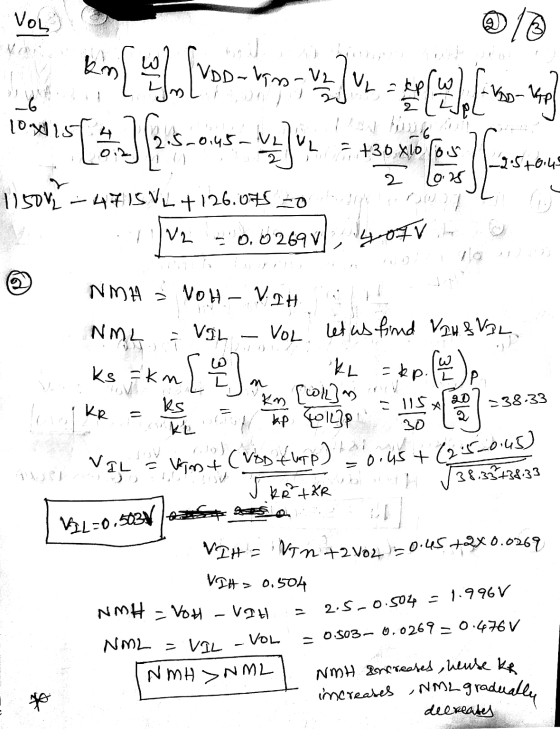
. Ratioed Logic, 25pts Consider a 4-input NOR gate implemented in pseudo-NMOS logic driving an in...
 . Ratioed Logic, 25pts Consider a 4-input NOR gate implemented in pseudo-NMOS logic driving an inverter with NM Vthn and NMH-Vthp. For the NOR gate, assume L -0.2μm for all transistors and W,-0.96μήη for the PMOS pull-up load transistor (input is connected to GND). Let VDo-1.2V. Use the parameters below for calculation. NMOS PMOS to 0.43 0.4 0.A 0.4 0.63 -1 115 -30 0.1 a) (9pts) Find the W of each NMOS (all sized equally) such that tpLH of the...
Consider the following current mirror combination, where all transistors have the same kn'(W/L) =...
 Consider the following current mirror
combination, where all transistors have the same
kn'(W/L) =
kp'(W/L) =
2mA/V2, and VTN =
1V, VTP = -1V. It is also given that VDD1 =
10V, VDD2 = 8V. Remember that for saturation the drain
current is given by ID = ½
kn'(W/L)
(VGS –
VTN)2 for NMOS and
ID = ½
kp'(W/L)
(VGS –
VTP)2 for PMOS. You can
ignore the channel modulation for all transistors.
Find the value of R so that...
Consider the following current mirror
combination, where all transistors have the same
kn'(W/L) =
kp'(W/L) =
2mA/V2, and VTN =
1V, VTP = -1V. It is also given that VDD1 =
10V, VDD2 = 8V. Remember that for saturation the drain
current is given by ID = ½
kn'(W/L)
(VGS –
VTN)2 for NMOS and
ID = ½
kp'(W/L)
(VGS –
VTP)2 for PMOS. You can
ignore the channel modulation for all transistors.
Find the value of R so that...
1. Consider the following current mirror combination, where all transistors have the same kn'(W/L...
 1. Consider the following current mirror combination, where all transistors have the same kn'(W/L) = kp'(W/L) = 2mA/V2, and VTN-1У, VTP--1V. It is also given that VDD1-10V, VDD2-8V. Remember that for saturation the drain current is given by IDー½ k,"(W/L) (VGS-Yn)" for NMOS and ID ½ kp"(WL) (VGS-V,»)2 for PMOS. You can ignore the channel modulation for all transistors. (a) Find the value of R so that I.-1mA. (b) Are transistors Q1, Q2, Q3 in saturation? (c) What is the...
 The following is the layout of an inverter with dimensions.
Assume that VDD=2.5V,
K’n=100uA/V2, Vtn=0.4V,
K’p=60uA/V2, Vtp=-0.5V,
tox=12nm, εox=3.9, Xd=42nm(overlap
distance under the gate), Cj=0.74fF/um2,
Cjsw=0.43fF/um for both NMOS and PMOS devices at zero
bias.
a.) Estimate the effective input capacitance of the inverter,
Cin.
b.) Estimate the effective output capacitance of the inverter,
Cout. For simplicity find effective Cout at
zero bias.
c.) If the output of this inverter is connected to a similar
inverter, estimate the tPHL and...
The following is the layout of an inverter with dimensions.
Assume that VDD=2.5V,
K’n=100uA/V2, Vtn=0.4V,
K’p=60uA/V2, Vtp=-0.5V,
tox=12nm, εox=3.9, Xd=42nm(overlap
distance under the gate), Cj=0.74fF/um2,
Cjsw=0.43fF/um for both NMOS and PMOS devices at zero
bias.
a.) Estimate the effective input capacitance of the inverter,
Cin.
b.) Estimate the effective output capacitance of the inverter,
Cout. For simplicity find effective Cout at
zero bias.
c.) If the output of this inverter is connected to a similar
inverter, estimate the tPHL and...
 . Ratioed Logic, 25pts Consider a 4-input NOR gate implemented in pseudo-NMOS logic driving an inverter with NM Vthn and NMH-Vthp. For the NOR gate, assume L -0.2μm for all transistors and W,-0.96μήη for the PMOS pull-up load transistor (input is connected to GND). Let VDo-1.2V. Use the parameters below for calculation. NMOS PMOS to 0.43 0.4 0.A 0.4 0.63 -1 115 -30 0.1 a) (9pts) Find the W of each NMOS (all sized equally) such that tpLH of the...
 Consider the following current mirror
combination, where all transistors have the same
kn'(W/L) =
kp'(W/L) =
2mA/V2, and VTN =
1V, VTP = -1V. It is also given that VDD1 =
10V, VDD2 = 8V. Remember that for saturation the drain
current is given by ID = ½
kn'(W/L)
(VGS –
VTN)2 for NMOS and
ID = ½
kp'(W/L)
(VGS –
VTP)2 for PMOS. You can
ignore the channel modulation for all transistors.
Find the value of R so that...
Consider the following current mirror
combination, where all transistors have the same
kn'(W/L) =
kp'(W/L) =
2mA/V2, and VTN =
1V, VTP = -1V. It is also given that VDD1 =
10V, VDD2 = 8V. Remember that for saturation the drain
current is given by ID = ½
kn'(W/L)
(VGS –
VTN)2 for NMOS and
ID = ½
kp'(W/L)
(VGS –
VTP)2 for PMOS. You can
ignore the channel modulation for all transistors.
Find the value of R so that...
 1. Consider the following current mirror combination, where all transistors have the same kn'(W/L) = kp'(W/L) = 2mA/V2, and VTN-1У, VTP--1V. It is also given that VDD1-10V, VDD2-8V. Remember that for saturation the drain current is given by IDー½ k,"(W/L) (VGS-Yn)" for NMOS and ID ½ kp"(WL) (VGS-V,»)2 for PMOS. You can ignore the channel modulation for all transistors. (a) Find the value of R so that I.-1mA. (b) Are transistors Q1, Q2, Q3 in saturation? (c) What is the...
Most questions answered within 3 hours.
-
Where is the error in this code sequence?
String s1 = "Hello";
String s2 = "ello";...
asked 10 months ago -
Financial data for Joel de Paris, Inc., for last year
follow:
Joel de Paris, Inc.
Balance...
asked 10 months ago -
Consider this reaction:
Al2(SO4)3 (aq)+ BaCl3
(aq) Al2Cl6 (aq)- +
3BaSO4(s) . What is the...
asked 10 months ago -
Suppose that Savneet is considering increasing her
recent random sample from 20 car rentals to 40...
asked 10 months ago -
Trucks arrive at an unloading terminal at an average rate of 120
per hour.
Trucks arrive...
asked 10 months ago -
Why are methanol and ethanol completely soluble in water while
octanol is not very little soluble....
asked 10 months ago -
A facilities manager at a university reads in a research report
that the mean amount of...
asked 10 months ago -
When the CuSO4 is rehydrated by adding water to the anhydrous
compound, is this an endothermic...
asked 10 months ago -
A ray of sunlight is passing from diamond into crown glass; the
angle of incidence is...
asked 10 months ago -
A block of mass 0.249 kg is placed on top of a light, vertical
spring of...
asked 10 months ago -
how do the kidneys compensate in the presences of acidosis
a) trigger hyperventilate
b) reserve acid...
asked 10 months ago -
Question 501 pts
The rental rate of capital to the firm increases. Which of the
following...
asked 10 months ago