
Homework Answers

Add Answer to:
results to verify your design. 2. For the circuit in Figure 2 calculate and select standard...
design a Voltage Divider Circuit that has the following – VCC= 12 V IC=2.5 mA ...
design a Voltage Divider Circuit that has the following – VCC= 12 V IC=2.5 mA VCE = 6 V For the design, you will use a 2n3904 npn transistor. Assume a β of 150. Determine values for RC, RE, R1, and R2
Please answer clearly 2. Consider the circuit shown in Figure 1. Determine values of Ri, R2, and Rc to provide the quie...
 Please answer clearly
2. Consider the circuit shown in Figure 1. Determine values of Ri, R2, and Rc to provide the quiescent emitter current 1.5 mA and the quiescent collector to emitter voltage 5V. Assume β 100, Re-I㏀、Va= 200V, VBEon-0.7V, and VT= 25mV. R1 Rc Vcc に 10v R2 Re Figure 1: BJT biasing configuration
2. Consider the circuit shown in Figure 1. Determine values of Ri, R2, and Rc to provide the quiescent emitter current 1.5 mA and the...
Please answer clearly
2. Consider the circuit shown in Figure 1. Determine values of Ri, R2, and Rc to provide the quiescent emitter current 1.5 mA and the quiescent collector to emitter voltage 5V. Assume β 100, Re-I㏀、Va= 200V, VBEon-0.7V, and VT= 25mV. R1 Rc Vcc に 10v R2 Re Figure 1: BJT biasing configuration
2. Consider the circuit shown in Figure 1. Determine values of Ri, R2, and Rc to provide the quiescent emitter current 1.5 mA and the...
Q. 3. Design a transistor biasing circuit as shown below. Assume B = 100, Ica =...
 Q. 3. Design a transistor biasing circuit as shown below. Assume B = 100, Ica = 10 mA, VE = Vcc/3, VceQ = Vcc /3 and VBE = 0.7 V. RTH = 0.1 (1 + B)RE . Also find the power rating of all resistors. (25) > +15V R2 Rc Vio R1 RE
Q. 3. Design a transistor biasing circuit as shown below. Assume ß = 100, lco =...
 Q. 3. Design a transistor biasing circuit as shown below. Assume ß = 100, lco = 10 mA, VE = Vcc/3, VCEQ = Vcc/3 and VBE = 0.7 V. RTH = 0.1 (1 + B)RE . Also find the power rating of all resistors. +15V R2 Rc V10 R1 RE
Design a transistor biasing circuit as shown below. Assume ß = 100, Ice = 10 mA,...
 Design a transistor biasing circuit as shown below. Assume ß = 100, Ice = 10 mA, VE = Vcc/3, VCEQ = Vcc/3 and VBE = 0.7 V. RTH = 0.1 (1 + BRE. Also find the power rating of all resistors. +15V R2 Rc V 10 R1 RE
could you please answer these 8 questions ? thnx VCC 15V Ic 1kQ RC R1 33KQ...
 could you please answer these 8 questions ? thnx
VCC 15V Ic 1kQ RC R1 33KQ VC C B 2N 5210 VB VBE VE R2 4700 RE ·10kΩ Refer to the data table for each of the following symptoms, choose one of the following faults as the most probable cause and write it in the space provided. POSSIBLE FAULTS R1 open Rc open RE decreased RE open R1 decreased R2 decreased R2 open Rc decreased Trouble in dc supply Transistor...
could you please answer these 8 questions ? thnx
VCC 15V Ic 1kQ RC R1 33KQ VC C B 2N 5210 VB VBE VE R2 4700 RE ·10kΩ Refer to the data table for each of the following symptoms, choose one of the following faults as the most probable cause and write it in the space provided. POSSIBLE FAULTS R1 open Rc open RE decreased RE open R1 decreased R2 decreased R2 open Rc decreased Trouble in dc supply Transistor...
VCC 24V RC 6.8kQ 100kΩ C2 0 15UF 01 C1 15uF 2N3904 R2 RE CE Figure 1. Common-emitter transistor a...
 Please use Multisim with probes placed and labeled.
Thank you for your time!
VCC 24V RC 6.8kQ 100kΩ C2 0 15UF 01 C1 15uF 2N3904 R2 RE CE Figure 1. Common-emitter transistor amplifier 2. Use Multisim to build circuit and measure the DC bias value for the figure above. 3. Calculate the AC dynamic resistance, re, using the measured value of lE 4. Calculate the amp voltage gain for the bypassed emitter 5. Record measured and calculated results in table...
Please use Multisim with probes placed and labeled.
Thank you for your time!
VCC 24V RC 6.8kQ 100kΩ C2 0 15UF 01 C1 15uF 2N3904 R2 RE CE Figure 1. Common-emitter transistor amplifier 2. Use Multisim to build circuit and measure the DC bias value for the figure above. 3. Calculate the AC dynamic resistance, re, using the measured value of lE 4. Calculate the amp voltage gain for the bypassed emitter 5. Record measured and calculated results in table...
[1] The circuit diagram on the left below is a common emitter amplifier. It is the...
 [1] The circuit diagram on the left below is a common emitter amplifier. It is the full complement of components for this type of amplifier ready for AC analysis. This amplifier will be discussed in lecture prior to the lab exercises. However, with the circuit including only Rc. RE, Ri, and R2 as shown in the figure on the right, proceed with the design for a DC operating point of the common emitter amplifier. The following parameters are given: Vcc...
Could someone please help me on how I should be configuring the circuit in Figure 4(a)...
 Could someone please help me on how I should be configuring the
circuit in Figure 4(a) in Multisim? Basically not understanding
question #1 in the Procedure. Cannot keep Vrb the same value while
adjusting Vcc. Then when trying to adjust Vbb to hold Vrb, Ib
changes.
Any help is appreciated!
Discrete Devices Section LAB 4 BJT CHARACTERISTICS AND BIASING Objective: The objective of this laboratory is to examine the operation of a bipolar junction transistor and plot its output characteristics...
Could someone please help me on how I should be configuring the
circuit in Figure 4(a) in Multisim? Basically not understanding
question #1 in the Procedure. Cannot keep Vrb the same value while
adjusting Vcc. Then when trying to adjust Vbb to hold Vrb, Ib
changes.
Any help is appreciated!
Discrete Devices Section LAB 4 BJT CHARACTERISTICS AND BIASING Objective: The objective of this laboratory is to examine the operation of a bipolar junction transistor and plot its output characteristics...
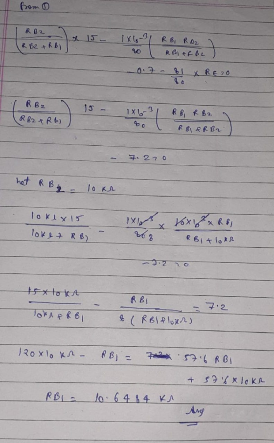
ECT2601/101/3/2019 TRANSISTOR BIAS CIRCUITS Question 2 Find lo. Vcn qnd V for the pnp transistor in...
 ECT2601/101/3/2019 TRANSISTOR BIAS CIRCUITS Question 2 Find lo. Vcn qnd V for the pnp transistor in figure 2 using the Thevenins Theorem applied o voltage divider Bias. (12) [12) VCC 12V IC Rc 3kQ R1 vc 04 2N5684G BDC 150 VB RE R2 30k0 1
 Please answer clearly
2. Consider the circuit shown in Figure 1. Determine values of Ri, R2, and Rc to provide the quiescent emitter current 1.5 mA and the quiescent collector to emitter voltage 5V. Assume β 100, Re-I㏀、Va= 200V, VBEon-0.7V, and VT= 25mV. R1 Rc Vcc に 10v R2 Re Figure 1: BJT biasing configuration
2. Consider the circuit shown in Figure 1. Determine values of Ri, R2, and Rc to provide the quiescent emitter current 1.5 mA and the...
Please answer clearly
2. Consider the circuit shown in Figure 1. Determine values of Ri, R2, and Rc to provide the quiescent emitter current 1.5 mA and the quiescent collector to emitter voltage 5V. Assume β 100, Re-I㏀、Va= 200V, VBEon-0.7V, and VT= 25mV. R1 Rc Vcc に 10v R2 Re Figure 1: BJT biasing configuration
2. Consider the circuit shown in Figure 1. Determine values of Ri, R2, and Rc to provide the quiescent emitter current 1.5 mA and the...
 Q. 3. Design a transistor biasing circuit as shown below. Assume B = 100, Ica = 10 mA, VE = Vcc/3, VceQ = Vcc /3 and VBE = 0.7 V. RTH = 0.1 (1 + B)RE . Also find the power rating of all resistors. (25) > +15V R2 Rc Vio R1 RE
 Q. 3. Design a transistor biasing circuit as shown below. Assume ß = 100, lco = 10 mA, VE = Vcc/3, VCEQ = Vcc/3 and VBE = 0.7 V. RTH = 0.1 (1 + B)RE . Also find the power rating of all resistors. +15V R2 Rc V10 R1 RE
 Design a transistor biasing circuit as shown below. Assume ß = 100, Ice = 10 mA, VE = Vcc/3, VCEQ = Vcc/3 and VBE = 0.7 V. RTH = 0.1 (1 + BRE. Also find the power rating of all resistors. +15V R2 Rc V 10 R1 RE
 could you please answer these 8 questions ? thnx
VCC 15V Ic 1kQ RC R1 33KQ VC C B 2N 5210 VB VBE VE R2 4700 RE ·10kΩ Refer to the data table for each of the following symptoms, choose one of the following faults as the most probable cause and write it in the space provided. POSSIBLE FAULTS R1 open Rc open RE decreased RE open R1 decreased R2 decreased R2 open Rc decreased Trouble in dc supply Transistor...
could you please answer these 8 questions ? thnx
VCC 15V Ic 1kQ RC R1 33KQ VC C B 2N 5210 VB VBE VE R2 4700 RE ·10kΩ Refer to the data table for each of the following symptoms, choose one of the following faults as the most probable cause and write it in the space provided. POSSIBLE FAULTS R1 open Rc open RE decreased RE open R1 decreased R2 decreased R2 open Rc decreased Trouble in dc supply Transistor...
 Please use Multisim with probes placed and labeled.
Thank you for your time!
VCC 24V RC 6.8kQ 100kΩ C2 0 15UF 01 C1 15uF 2N3904 R2 RE CE Figure 1. Common-emitter transistor amplifier 2. Use Multisim to build circuit and measure the DC bias value for the figure above. 3. Calculate the AC dynamic resistance, re, using the measured value of lE 4. Calculate the amp voltage gain for the bypassed emitter 5. Record measured and calculated results in table...
Please use Multisim with probes placed and labeled.
Thank you for your time!
VCC 24V RC 6.8kQ 100kΩ C2 0 15UF 01 C1 15uF 2N3904 R2 RE CE Figure 1. Common-emitter transistor amplifier 2. Use Multisim to build circuit and measure the DC bias value for the figure above. 3. Calculate the AC dynamic resistance, re, using the measured value of lE 4. Calculate the amp voltage gain for the bypassed emitter 5. Record measured and calculated results in table...
 [1] The circuit diagram on the left below is a common emitter amplifier. It is the full complement of components for this type of amplifier ready for AC analysis. This amplifier will be discussed in lecture prior to the lab exercises. However, with the circuit including only Rc. RE, Ri, and R2 as shown in the figure on the right, proceed with the design for a DC operating point of the common emitter amplifier. The following parameters are given: Vcc...
 Could someone please help me on how I should be configuring the
circuit in Figure 4(a) in Multisim? Basically not understanding
question #1 in the Procedure. Cannot keep Vrb the same value while
adjusting Vcc. Then when trying to adjust Vbb to hold Vrb, Ib
changes.
Any help is appreciated!
Discrete Devices Section LAB 4 BJT CHARACTERISTICS AND BIASING Objective: The objective of this laboratory is to examine the operation of a bipolar junction transistor and plot its output characteristics...
Could someone please help me on how I should be configuring the
circuit in Figure 4(a) in Multisim? Basically not understanding
question #1 in the Procedure. Cannot keep Vrb the same value while
adjusting Vcc. Then when trying to adjust Vbb to hold Vrb, Ib
changes.
Any help is appreciated!
Discrete Devices Section LAB 4 BJT CHARACTERISTICS AND BIASING Objective: The objective of this laboratory is to examine the operation of a bipolar junction transistor and plot its output characteristics...
 ECT2601/101/3/2019 TRANSISTOR BIAS CIRCUITS Question 2 Find lo. Vcn qnd V for the pnp transistor in figure 2 using the Thevenins Theorem applied o voltage divider Bias. (12) [12) VCC 12V IC Rc 3kQ R1 vc 04 2N5684G BDC 150 VB RE R2 30k0 1
Most questions answered within 3 hours.
-
Where is the error in this code sequence?
String s1 = "Hello";
String s2 = "ello";...
asked 10 months ago -
Financial data for Joel de Paris, Inc., for last year
follow:
Joel de Paris, Inc.
Balance...
asked 10 months ago -
Consider this reaction:
Al2(SO4)3 (aq)+ BaCl3
(aq) Al2Cl6 (aq)- +
3BaSO4(s) . What is the...
asked 10 months ago -
Suppose that Savneet is considering increasing her
recent random sample from 20 car rentals to 40...
asked 10 months ago -
Trucks arrive at an unloading terminal at an average rate of 120
per hour.
Trucks arrive...
asked 10 months ago -
Why are methanol and ethanol completely soluble in water while
octanol is not very little soluble....
asked 10 months ago -
A facilities manager at a university reads in a research report
that the mean amount of...
asked 10 months ago -
When the CuSO4 is rehydrated by adding water to the anhydrous
compound, is this an endothermic...
asked 10 months ago -
A ray of sunlight is passing from diamond into crown glass; the
angle of incidence is...
asked 10 months ago -
A block of mass 0.249 kg is placed on top of a light, vertical
spring of...
asked 10 months ago -
how do the kidneys compensate in the presences of acidosis
a) trigger hyperventilate
b) reserve acid...
asked 10 months ago -
Question 501 pts
The rental rate of capital to the firm increases. Which of the
following...
asked 10 months ago