The circuit below is "Differential amplifier" The waveform of
the input signal is shown below. The input signal is 
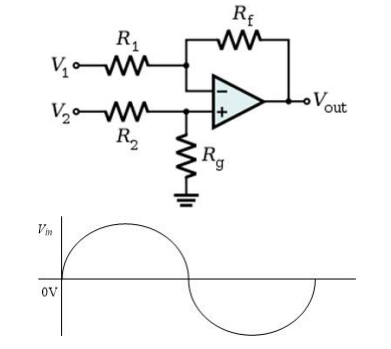
(1) An expression of the gain of a closed loop on a circuit

Use to induce. (formerly op-amp)
The analysis method can be used. KVL and KCL can be utilized
properly.)
(2)When  set the resistance value so that the closed loop gain is 2.5 and
the output synchronized with the input signal.
set the resistance value so that the closed loop gain is 2.5 and
the output synchronized with the input signal.
Sketch the force signal (exactly mark the maximum and minimum
values and cycles of the output signal on the output signal
waveform).
Homework Answers


Add Answer to:
The circuit below is "Differential amplifier" The waveform of
the input signal is shown below. The...
Read the question carefully and please answer it fully knowing that the input voltages do not hav...
 Read the question carefully and please answer it fully knowing
that the input voltages do not have the same frequency. If you are
unable to answer any part of the question, please leave it for
someone else.
Question: Consider the following summing amplifier. Let all
resistors be of value (33000 ohms) and
Vin1 is a 1 kHz sinusoidal waveform with peak to
peak voltage of 1 volt, Vin2 is a 100 Hz
sinusoidal waveform with peak to peak voltage of...
Read the question carefully and please answer it fully knowing
that the input voltages do not have the same frequency. If you are
unable to answer any part of the question, please leave it for
someone else.
Question: Consider the following summing amplifier. Let all
resistors be of value (33000 ohms) and
Vin1 is a 1 kHz sinusoidal waveform with peak to
peak voltage of 1 volt, Vin2 is a 100 Hz
sinusoidal waveform with peak to peak voltage of...
Consider the common-emitter amplifier in the following figure, with = 100, VA = 100V, C= 25fF,...
 Consider the common-emitter amplifier in the following figure,
with = 100,
VA = 100V, C= 25fF,
C= 10fF.
a) Draw the small-signal model of this circuit. Apply Miller’s
theorem to split C to input and
output nodes. Calculate the time constants at the input and output
nodes, in and
out.
b) Based on the time constants from part a), calculate the input
and output pole frequencies, fin and fout.
What is the dominant pole of this amplifier?
We were unable...
Consider the common-emitter amplifier in the following figure,
with = 100,
VA = 100V, C= 25fF,
C= 10fF.
a) Draw the small-signal model of this circuit. Apply Miller’s
theorem to split C to input and
output nodes. Calculate the time constants at the input and output
nodes, in and
out.
b) Based on the time constants from part a), calculate the input
and output pole frequencies, fin and fout.
What is the dominant pole of this amplifier?
We were unable...
V1 R2 RG R1 Vout R3 2 o FIGURE 37 This instrumentation amplifier allows the gain to be changed us...
 V1 R2 RG R1 Vout R3 2 o FIGURE 37 This instrumentation amplifier allows the gain to be changed using a single resistor. We were unable to transcribe this image
V1 R2 RG R1 Vout R3 2 o FIGURE 37 This instrumentation amplifier allows the gain to be changed using a single resistor.
V1 R2 RG R1 Vout R3 2 o FIGURE 37 This instrumentation amplifier allows the gain to be changed using a single resistor. We were unable to transcribe this image
V1 R2 RG R1 Vout R3 2 o FIGURE 37 This instrumentation amplifier allows the gain to be changed using a single resistor.
6.57 An alternative equivalent circuit of an amplifier fed with a signal source (Urie, Ric) and...
 6.57 An alternative equivalent circuit of an amplifier fed with a signal source (Urie, Ric) and connected to a load R, is shown in Fig. P6.57. Here Gy is the open-circuit overall voltage gain, Con = 1 and Rour is the output resistance with Usie set to zero. This is different than R. Show that 6,10 AJO R + Rsig where R;= Rine, a Also show that the overall voltage gain is G., Cvo R+ Roul We were unable to...
A MOSFET is wired as a common-source amplifier as shown below. The input voltage vIN is...
 A MOSFET is wired as a common-source amplifier as shown below.
The input voltage vIN is the total of the source for
biasing the circuit at its operating point (vBIAS), and
a small signal ac source providing the signal that we want to
amplify (vin). The total output voltage is
vO.
a) Assume VDD = 5?, VIN = 2?, and ? = 4?Ω
in the circuit and the MOSFET parameters are K =
0.5??/?2, VTH 1?, and ? = 0.05V-1....
A MOSFET is wired as a common-source amplifier as shown below.
The input voltage vIN is the total of the source for
biasing the circuit at its operating point (vBIAS), and
a small signal ac source providing the signal that we want to
amplify (vin). The total output voltage is
vO.
a) Assume VDD = 5?, VIN = 2?, and ? = 4?Ω
in the circuit and the MOSFET parameters are K =
0.5??/?2, VTH 1?, and ? = 0.05V-1....
1. The feedback is negative. True or False? 2. Find the value of the forward amplifier...
 1. The feedback is negative. True or
False?
2. Find the value of the forward amplifier gain
3. If R1=10kΩ, what value should R2 have to have a feedback
factor of 1/2?
4. The closed-loop gain is about …
(Hint: The closed-loop gain is positive)
A) 1.5
B) 2.8
C) 1.9
D) 3.7
5) If the overall forward amplifier has a 150 Hz bandwidth (due
to a single dominant pole), the bandwidth of the closed-loop
circuit would be around …...
1. The feedback is negative. True or
False?
2. Find the value of the forward amplifier gain
3. If R1=10kΩ, what value should R2 have to have a feedback
factor of 1/2?
4. The closed-loop gain is about …
(Hint: The closed-loop gain is positive)
A) 1.5
B) 2.8
C) 1.9
D) 3.7
5) If the overall forward amplifier has a 150 Hz bandwidth (due
to a single dominant pole), the bandwidth of the closed-loop
circuit would be around …...
4. A sinusoidal signal was used as the input to the inverting amplifier below. The op...
 4. A sinusoidal signal was used as the input to the inverting amplifier below. The op amp is ideal except for its open-loop gain. It has an open loop de gain (Ao) of 100dB and a unity-gain bandwidth (f) of 100 MHz. a) Find the transfer function, H(o), including the non-ideal open loop gain, A. b) Find the 3-dB frequency for the op amp, and sketch the |Al vs. frequency graph. Label the open loop de gain, 3-dB frequency, and...
3- OPERATIONAL-AMPLIFIER Nominating ampliar Voltage Show OW Difference ampliar Wate Date amplizier Close R Vout Voutin...
 3- OPERATIONAL-AMPLIFIER Nominating ampliar Voltage Show OW Difference ampliar Wate Date amplizier Close R Vout Voutin Vout = vin Buffer = Inverting amplifier Dout = (1 + .. Vout V out 1 V2 ERR Vour (, - v3) Differential Amplifier Non-Inverting amplifier 1- Refer to the op amp in Fig. If v; = 0.5 V, calculate: (a) the output voltage Vos (b) the current in the 10-k! resistor. 25k92 10k02 Oo + 6 2. A 741 op amp has an...
A. (10 pts) Implement the voltage amplifier shown below using an ideal op amp circuit. You have o...
 a. (10 pts) Implement the voltage amplifier shown below using an ideal op amp circuit. You have one op amp available for this circuit, and a range of resistors with values from 1 kΩ to 100 ka. Draw the schematic of your op amp circuit, labeling resistor values. Make sure the gain, input resistance, and output resistance of your circuit matches the model in the schematic. R=012 *100v, RL 100 b. (5 pts) Your amplifier circuit should have a frequency...
Figure 2 shows a feedback amplifier circuit. Rs is the source resistor and R, is the...
 Figure 2 shows a feedback amplifier circuit. Rs is the source resistor and R, is the load resistor RS Vs VI RL OPAMP R2 R1 RM R3 R4 Step 1: open-loop and closed-loop circuits identification 1.1 Identify the source, the load, and the closed-loop amplifier 1.2 Identify the open-loop amplifier (**A" eireuit) and the feedback network (B" eircuit) in the closed-loop amplifier 1.3 Identify the connection type between the "A" circuit and the "B" circuit at both the input and...
 Read the question carefully and please answer it fully knowing
that the input voltages do not have the same frequency. If you are
unable to answer any part of the question, please leave it for
someone else.
Question: Consider the following summing amplifier. Let all
resistors be of value (33000 ohms) and
Vin1 is a 1 kHz sinusoidal waveform with peak to
peak voltage of 1 volt, Vin2 is a 100 Hz
sinusoidal waveform with peak to peak voltage of...
Read the question carefully and please answer it fully knowing
that the input voltages do not have the same frequency. If you are
unable to answer any part of the question, please leave it for
someone else.
Question: Consider the following summing amplifier. Let all
resistors be of value (33000 ohms) and
Vin1 is a 1 kHz sinusoidal waveform with peak to
peak voltage of 1 volt, Vin2 is a 100 Hz
sinusoidal waveform with peak to peak voltage of...
 Consider the common-emitter amplifier in the following figure,
with = 100,
VA = 100V, C= 25fF,
C= 10fF.
a) Draw the small-signal model of this circuit. Apply Miller’s
theorem to split C to input and
output nodes. Calculate the time constants at the input and output
nodes, in and
out.
b) Based on the time constants from part a), calculate the input
and output pole frequencies, fin and fout.
What is the dominant pole of this amplifier?
We were unable...
Consider the common-emitter amplifier in the following figure,
with = 100,
VA = 100V, C= 25fF,
C= 10fF.
a) Draw the small-signal model of this circuit. Apply Miller’s
theorem to split C to input and
output nodes. Calculate the time constants at the input and output
nodes, in and
out.
b) Based on the time constants from part a), calculate the input
and output pole frequencies, fin and fout.
What is the dominant pole of this amplifier?
We were unable...
 V1 R2 RG R1 Vout R3 2 o FIGURE 37 This instrumentation amplifier allows the gain to be changed using a single resistor. We were unable to transcribe this image
V1 R2 RG R1 Vout R3 2 o FIGURE 37 This instrumentation amplifier allows the gain to be changed using a single resistor.
V1 R2 RG R1 Vout R3 2 o FIGURE 37 This instrumentation amplifier allows the gain to be changed using a single resistor. We were unable to transcribe this image
V1 R2 RG R1 Vout R3 2 o FIGURE 37 This instrumentation amplifier allows the gain to be changed using a single resistor.
 6.57 An alternative equivalent circuit of an amplifier fed with a signal source (Urie, Ric) and connected to a load R, is shown in Fig. P6.57. Here Gy is the open-circuit overall voltage gain, Con = 1 and Rour is the output resistance with Usie set to zero. This is different than R. Show that 6,10 AJO R + Rsig where R;= Rine, a Also show that the overall voltage gain is G., Cvo R+ Roul We were unable to...
 A MOSFET is wired as a common-source amplifier as shown below.
The input voltage vIN is the total of the source for
biasing the circuit at its operating point (vBIAS), and
a small signal ac source providing the signal that we want to
amplify (vin). The total output voltage is
vO.
a) Assume VDD = 5?, VIN = 2?, and ? = 4?Ω
in the circuit and the MOSFET parameters are K =
0.5??/?2, VTH 1?, and ? = 0.05V-1....
A MOSFET is wired as a common-source amplifier as shown below.
The input voltage vIN is the total of the source for
biasing the circuit at its operating point (vBIAS), and
a small signal ac source providing the signal that we want to
amplify (vin). The total output voltage is
vO.
a) Assume VDD = 5?, VIN = 2?, and ? = 4?Ω
in the circuit and the MOSFET parameters are K =
0.5??/?2, VTH 1?, and ? = 0.05V-1....
 1. The feedback is negative. True or
False?
2. Find the value of the forward amplifier gain
3. If R1=10kΩ, what value should R2 have to have a feedback
factor of 1/2?
4. The closed-loop gain is about …
(Hint: The closed-loop gain is positive)
A) 1.5
B) 2.8
C) 1.9
D) 3.7
5) If the overall forward amplifier has a 150 Hz bandwidth (due
to a single dominant pole), the bandwidth of the closed-loop
circuit would be around …...
1. The feedback is negative. True or
False?
2. Find the value of the forward amplifier gain
3. If R1=10kΩ, what value should R2 have to have a feedback
factor of 1/2?
4. The closed-loop gain is about …
(Hint: The closed-loop gain is positive)
A) 1.5
B) 2.8
C) 1.9
D) 3.7
5) If the overall forward amplifier has a 150 Hz bandwidth (due
to a single dominant pole), the bandwidth of the closed-loop
circuit would be around …...
 4. A sinusoidal signal was used as the input to the inverting amplifier below. The op amp is ideal except for its open-loop gain. It has an open loop de gain (Ao) of 100dB and a unity-gain bandwidth (f) of 100 MHz. a) Find the transfer function, H(o), including the non-ideal open loop gain, A. b) Find the 3-dB frequency for the op amp, and sketch the |Al vs. frequency graph. Label the open loop de gain, 3-dB frequency, and...
 3- OPERATIONAL-AMPLIFIER Nominating ampliar Voltage Show OW Difference ampliar Wate Date amplizier Close R Vout Voutin Vout = vin Buffer = Inverting amplifier Dout = (1 + .. Vout V out 1 V2 ERR Vour (, - v3) Differential Amplifier Non-Inverting amplifier 1- Refer to the op amp in Fig. If v; = 0.5 V, calculate: (a) the output voltage Vos (b) the current in the 10-k! resistor. 25k92 10k02 Oo + 6 2. A 741 op amp has an...
 a. (10 pts) Implement the voltage amplifier shown below using an ideal op amp circuit. You have one op amp available for this circuit, and a range of resistors with values from 1 kΩ to 100 ka. Draw the schematic of your op amp circuit, labeling resistor values. Make sure the gain, input resistance, and output resistance of your circuit matches the model in the schematic. R=012 *100v, RL 100 b. (5 pts) Your amplifier circuit should have a frequency...
 Figure 2 shows a feedback amplifier circuit. Rs is the source resistor and R, is the load resistor RS Vs VI RL OPAMP R2 R1 RM R3 R4 Step 1: open-loop and closed-loop circuits identification 1.1 Identify the source, the load, and the closed-loop amplifier 1.2 Identify the open-loop amplifier (**A" eireuit) and the feedback network (B" eircuit) in the closed-loop amplifier 1.3 Identify the connection type between the "A" circuit and the "B" circuit at both the input and...
Most questions answered within 3 hours.
-
Where is the error in this code sequence?
String s1 = "Hello";
String s2 = "ello";...
asked 10 months ago -
Financial data for Joel de Paris, Inc., for last year
follow:
Joel de Paris, Inc.
Balance...
asked 10 months ago -
Consider this reaction:
Al2(SO4)3 (aq)+ BaCl3
(aq) Al2Cl6 (aq)- +
3BaSO4(s) . What is the...
asked 10 months ago -
Suppose that Savneet is considering increasing her
recent random sample from 20 car rentals to 40...
asked 10 months ago -
Trucks arrive at an unloading terminal at an average rate of 120
per hour.
Trucks arrive...
asked 10 months ago -
Why are methanol and ethanol completely soluble in water while
octanol is not very little soluble....
asked 10 months ago -
A facilities manager at a university reads in a research report
that the mean amount of...
asked 10 months ago -
When the CuSO4 is rehydrated by adding water to the anhydrous
compound, is this an endothermic...
asked 10 months ago -
A ray of sunlight is passing from diamond into crown glass; the
angle of incidence is...
asked 10 months ago -
A block of mass 0.249 kg is placed on top of a light, vertical
spring of...
asked 10 months ago -
how do the kidneys compensate in the presences of acidosis
a) trigger hyperventilate
b) reserve acid...
asked 10 months ago -
Question 501 pts
The rental rate of capital to the firm increases. Which of the
following...
asked 10 months ago