
Homework Answers


Add Answer to:
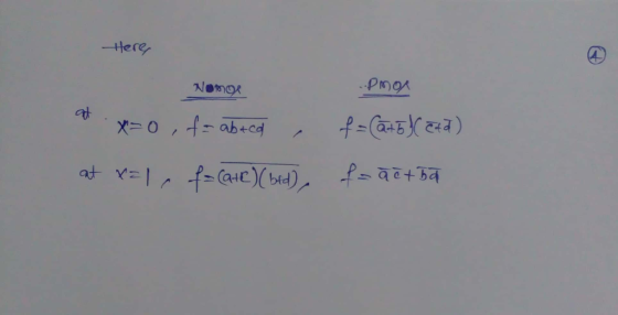
(Pull-Up/Pull-Down Network in CMOS gates - 20 points) Consider the pull-down network (consisting of NMOS transistors)...
3. (20 points). A CMOS logic circuit is a generalization of the CMOS inverter. CMOS employs MOS t...
 3. (20 points). A CMOS logic circuit is a generalization of the CMOS inverter. CMOS employs MOS transistors of both polarities. a) In Fig. 3 indicate NMOS and PMOS transistors; b) The inverter consists of an NMOS pulldown and PMOS pull-up transistor. Draw the CMOS NOT gate. Gate Gate Oxlde Oxlde Fig.3
3. (20 points). A CMOS logic circuit is a generalization of the CMOS inverter. CMOS employs MOS transistors of both polarities. a) In Fig. 3 indicate NMOS and...
3. (20 points). A CMOS logic circuit is a generalization of the CMOS inverter. CMOS employs MOS transistors of both polarities. a) In Fig. 3 indicate NMOS and PMOS transistors; b) The inverter consists of an NMOS pulldown and PMOS pull-up transistor. Draw the CMOS NOT gate. Gate Gate Oxlde Oxlde Fig.3
3. (20 points). A CMOS logic circuit is a generalization of the CMOS inverter. CMOS employs MOS transistors of both polarities. a) In Fig. 3 indicate NMOS and...
CMOS Design Styles Quiz Problem 1: a) What is the typical "topology" for pMOS and nMOS...
CMOS Design Styles Quiz Problem 1: a) What is the typical "topology" for pMOS and nMOS in digital circuitry? -pMOS Vdd to Vout, nMOS Vout to Gnd -nMOS Vdd to Vout, pMOS Vout to Gnd -pMOS Vdd to Gnd, nMOS Vin to Vout -Only use xMOS -Both transistors Vin to Vout b) How do you implement nMOS in AND functions? -series connected, with increased widths -Parallel connected, with standard widths -Series connected with half the widths -Parallel connected, alternating large...
Design a Full subtractor in static CMOS technology. Include logic equations, pull up/pull down networks and stick diagrams
Design a Full subtractor in static CMOS technology. Include logic equations, pull up/pull down networks and stick diagrams
1. (30 pts) The pull up network (PUN) is provided for the CMOS logic gate below....
 1. (30 pts) The pull up network (PUN) is provided for the CMOS logic gate below. 8 Voo Quo EL Pull Down Network a) (10 pts) Sketch the equivalent pull down network (PDN). b) (10 pts) If each transistor in the gate has a length of Lmin, select gate widths in microns) for each p-channel transistor based on best practice sizing principles and referenced to the minimum sized inverter in the technology. W OpA = Lim WOD = um WOpB...
 3. (20 points). A CMOS logic circuit is a generalization of the CMOS inverter. CMOS employs MOS transistors of both polarities. a) In Fig. 3 indicate NMOS and PMOS transistors; b) The inverter consists of an NMOS pulldown and PMOS pull-up transistor. Draw the CMOS NOT gate. Gate Gate Oxlde Oxlde Fig.3
3. (20 points). A CMOS logic circuit is a generalization of the CMOS inverter. CMOS employs MOS transistors of both polarities. a) In Fig. 3 indicate NMOS and...
3. (20 points). A CMOS logic circuit is a generalization of the CMOS inverter. CMOS employs MOS transistors of both polarities. a) In Fig. 3 indicate NMOS and PMOS transistors; b) The inverter consists of an NMOS pulldown and PMOS pull-up transistor. Draw the CMOS NOT gate. Gate Gate Oxlde Oxlde Fig.3
3. (20 points). A CMOS logic circuit is a generalization of the CMOS inverter. CMOS employs MOS transistors of both polarities. a) In Fig. 3 indicate NMOS and...
 1. (30 pts) The pull up network (PUN) is provided for the CMOS logic gate below. 8 Voo Quo EL Pull Down Network a) (10 pts) Sketch the equivalent pull down network (PDN). b) (10 pts) If each transistor in the gate has a length of Lmin, select gate widths in microns) for each p-channel transistor based on best practice sizing principles and referenced to the minimum sized inverter in the technology. W OpA = Lim WOD = um WOpB...
Most questions answered within 3 hours.
-
Where is the error in this code sequence?
String s1 = "Hello";
String s2 = "ello";...
asked 11 months ago -
Financial data for Joel de Paris, Inc., for last year
follow:
Joel de Paris, Inc.
Balance...
asked 11 months ago -
Consider this reaction:
Al2(SO4)3 (aq)+ BaCl3
(aq) Al2Cl6 (aq)- +
3BaSO4(s) . What is the...
asked 11 months ago -
Suppose that Savneet is considering increasing her
recent random sample from 20 car rentals to 40...
asked 11 months ago -
Trucks arrive at an unloading terminal at an average rate of 120
per hour.
Trucks arrive...
asked 11 months ago -
Why are methanol and ethanol completely soluble in water while
octanol is not very little soluble....
asked 11 months ago -
A facilities manager at a university reads in a research report
that the mean amount of...
asked 11 months ago -
When the CuSO4 is rehydrated by adding water to the anhydrous
compound, is this an endothermic...
asked 11 months ago -
A ray of sunlight is passing from diamond into crown glass; the
angle of incidence is...
asked 11 months ago -
A block of mass 0.249 kg is placed on top of a light, vertical
spring of...
asked 11 months ago -
how do the kidneys compensate in the presences of acidosis
a) trigger hyperventilate
b) reserve acid...
asked 11 months ago -
Question 501 pts
The rental rate of capital to the firm increases. Which of the
following...
asked 11 months ago