For 4 by 4 multiplier, the circuit complexity is given by a. 16 FAs, and 16...
For 4 by 4 multiplier, the circuit complexity is given by
a. 16 FAs, and 16 AND gates
b. 12 FAs and 16 AND gates
c. 8 FAs and 12 gates.
Homework Answers
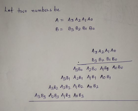
We can see 16 product terms and hence 16 AND gates needed.
Now to add up partial products and carry propagated from each addition is used for addition of next higher product bit, we need 12 adders (Half and Full Adders)
Hence option (b) is most appropriate answer.
Add Answer to:
For 4 by 4 multiplier, the circuit complexity is given by
a. 16 FAs, and 16...
Make a 4-to-16 decoder and show its circuit diagram in both ways: -Create every minterm via...
Make a 4-to-16 decoder and show its circuit diagram in both ways: -Create every minterm via multiple 4-input AND gates. -Employ hierarchical design, use smaller decoders and two groups of 8 AND gates.
Given the following Karnaugh map AB CD 00 01 11 10 01 011 Draw a circuit...
 Given the following Karnaugh map AB CD 00 01 11 10 01 011 Draw a circuit that realizes the function above using one 8-to-1 multiplexer and any number of NAND gates. Observe that A, B and C are connected to the select inputs, SO, S1, and S2. 4-to-1 MUX -10 12 13 14 15 16 17 So Si S2 ABC
Vhdl language PROJECT REQUIREMENT Design 8*8 bit signed multiplier A*B circuit using Booth Multiplier (you will...
 Vhdl language
PROJECT REQUIREMENT Design 8*8 bit signed multiplier A*B circuit using Booth Multiplier (you will learn about this in the course). . A and B are 8-bits signed numbers. . The operands A and B must be written into registers RA and RB on the negative edge of the LOAD flag. Output of the multiplier is a 16 bit register Z . The project must be written in structural VHDL mode, Each component Implementation and simulation details should be...
Vhdl language
PROJECT REQUIREMENT Design 8*8 bit signed multiplier A*B circuit using Booth Multiplier (you will learn about this in the course). . A and B are 8-bits signed numbers. . The operands A and B must be written into registers RA and RB on the negative edge of the LOAD flag. Output of the multiplier is a 16 bit register Z . The project must be written in structural VHDL mode, Each component Implementation and simulation details should be...
Class 24 1. Given the shorthand POS expression F(a,b,c,d) П M (0,6,7,8) (b + c + d)(a + D+ ē): a....
 Class 24 1. Given the shorthand POS expression F(a,b,c,d) П M (0,6,7,8) (b + c + d)(a + D+ ē): a. (25 points) Implement F using one 4-to-16 decoder and one OR gate of any size. b. (25 points) Implement F using four 2-40-4 decoders and one OR gate of any size. c. (25 points) Implement F using just two 8-to-3 encoders, NOT gates, and one AND gate of any size. Hint: given NOT gates and an AND gate to...
6) For following multiplier circuit, calculate the process time if: Td (carry) 2ns, Td (sum) -2ns,...
 6) For following multiplier circuit, calculate the process time if: Td (carry) 2ns, Td (sum) -2ns, Td (gate) ns, Td (each shit operation) = 10ns, only input logic two gates are available. a. Ripple carry adder used in ALU Carry Look Ahead used in ALU Multiplicand 32 bits 32-bit ALU Shift right Write Control Product test 64 bits
6) For following multiplier circuit, calculate the process time if: Td (carry) 2ns, Td (sum) -2ns, Td (gate) ns, Td (each shit...
6) For following multiplier circuit, calculate the process time if: Td (carry) 2ns, Td (sum) -2ns, Td (gate) ns, Td (each shit operation) = 10ns, only input logic two gates are available. a. Ripple carry adder used in ALU Carry Look Ahead used in ALU Multiplicand 32 bits 32-bit ALU Shift right Write Control Product test 64 bits
6) For following multiplier circuit, calculate the process time if: Td (carry) 2ns, Td (sum) -2ns, Td (gate) ns, Td (each shit...
Which of the following triggers apoptosis? a. Fas ligand b. NGF c. TNF-alpha d. Fas ligand...
Which of the following triggers apoptosis? a. Fas ligand b. NGF c. TNF-alpha d. Fas ligand and TNF-alpha e. Capase 8
Create a 4 bit Signed Multiplier with the following specifications: INPUTS A 4 bit 2's complement...
 Create a 4 bit Signed Multiplier with the following specifications: INPUTS A 4 bit 2's complement binary number. This could be positive or negative. B 4 bit 2's complement binary number. This could be positive or negative OUTPUT: 8 bit 2's complement binary number (This could be a positive or negative number) The overall circuit should look like this: 2's Complement Signed Multiplier At a minimum, the circuit must be implemented using controlled inverters and an unsigned multiplier as discussed...
ame. QUESTION 3 4 x 4 = 16 points Design a circuit that generates the 9's...
 ame. QUESTION 3 4 x 4 = 16 points Design a circuit that generates the 9's complement of a binary-coded decimal (BCD) digit. ABCD is a type of binary representation for decimal values (0 to 9) where each digit is represented by a fixed number of binary bits (use Tour bits for this problem). Note that the 9's complement of d is 9 d. (0) Show the corresponding truth table. Write down the functional relationship among the variables (outputs in...
4) Parity Design Circuit. 15 pts. a) Design a circuit that will give a "" if...
 4) Parity Design Circuit. 15 pts. a) Design a circuit that will give a "" if the four data lines into the circuit have an ODD parity. You may use any combination two input coincidence gates and/or two input exclusive OR gates. b) Redesign the circuit replacing the coincidence and exclusive OR gates with any combination of invertors, two input NAND and two input NOR. c) Each NAND, NOR or invertor has a 10nS propagation delay. Determine the worst case...
In the circuit given below, R 16 Ω. Determine Vo. 40 V(+ 10Ω 4 1 The...
 In the circuit given below, R 16 Ω. Determine Vo. 40 V(+ 10Ω 4 1 The equation at node Vy is: where A Click to select) B (Click to select) and c Click to select) The equation at node Vo is: where D(Click to select) and E (Click to select) v The value of Vo in the circuit is V.
 Given the following Karnaugh map AB CD 00 01 11 10 01 011 Draw a circuit that realizes the function above using one 8-to-1 multiplexer and any number of NAND gates. Observe that A, B and C are connected to the select inputs, SO, S1, and S2. 4-to-1 MUX -10 12 13 14 15 16 17 So Si S2 ABC
 Vhdl language
PROJECT REQUIREMENT Design 8*8 bit signed multiplier A*B circuit using Booth Multiplier (you will learn about this in the course). . A and B are 8-bits signed numbers. . The operands A and B must be written into registers RA and RB on the negative edge of the LOAD flag. Output of the multiplier is a 16 bit register Z . The project must be written in structural VHDL mode, Each component Implementation and simulation details should be...
Vhdl language
PROJECT REQUIREMENT Design 8*8 bit signed multiplier A*B circuit using Booth Multiplier (you will learn about this in the course). . A and B are 8-bits signed numbers. . The operands A and B must be written into registers RA and RB on the negative edge of the LOAD flag. Output of the multiplier is a 16 bit register Z . The project must be written in structural VHDL mode, Each component Implementation and simulation details should be...
 Class 24 1. Given the shorthand POS expression F(a,b,c,d) П M (0,6,7,8) (b + c + d)(a + D+ ē): a. (25 points) Implement F using one 4-to-16 decoder and one OR gate of any size. b. (25 points) Implement F using four 2-40-4 decoders and one OR gate of any size. c. (25 points) Implement F using just two 8-to-3 encoders, NOT gates, and one AND gate of any size. Hint: given NOT gates and an AND gate to...
 6) For following multiplier circuit, calculate the process time if: Td (carry) 2ns, Td (sum) -2ns, Td (gate) ns, Td (each shit operation) = 10ns, only input logic two gates are available. a. Ripple carry adder used in ALU Carry Look Ahead used in ALU Multiplicand 32 bits 32-bit ALU Shift right Write Control Product test 64 bits
6) For following multiplier circuit, calculate the process time if: Td (carry) 2ns, Td (sum) -2ns, Td (gate) ns, Td (each shit...
6) For following multiplier circuit, calculate the process time if: Td (carry) 2ns, Td (sum) -2ns, Td (gate) ns, Td (each shit operation) = 10ns, only input logic two gates are available. a. Ripple carry adder used in ALU Carry Look Ahead used in ALU Multiplicand 32 bits 32-bit ALU Shift right Write Control Product test 64 bits
6) For following multiplier circuit, calculate the process time if: Td (carry) 2ns, Td (sum) -2ns, Td (gate) ns, Td (each shit...
 Create a 4 bit Signed Multiplier with the following specifications: INPUTS A 4 bit 2's complement binary number. This could be positive or negative. B 4 bit 2's complement binary number. This could be positive or negative OUTPUT: 8 bit 2's complement binary number (This could be a positive or negative number) The overall circuit should look like this: 2's Complement Signed Multiplier At a minimum, the circuit must be implemented using controlled inverters and an unsigned multiplier as discussed...
 ame. QUESTION 3 4 x 4 = 16 points Design a circuit that generates the 9's complement of a binary-coded decimal (BCD) digit. ABCD is a type of binary representation for decimal values (0 to 9) where each digit is represented by a fixed number of binary bits (use Tour bits for this problem). Note that the 9's complement of d is 9 d. (0) Show the corresponding truth table. Write down the functional relationship among the variables (outputs in...
 4) Parity Design Circuit. 15 pts. a) Design a circuit that will give a "" if the four data lines into the circuit have an ODD parity. You may use any combination two input coincidence gates and/or two input exclusive OR gates. b) Redesign the circuit replacing the coincidence and exclusive OR gates with any combination of invertors, two input NAND and two input NOR. c) Each NAND, NOR or invertor has a 10nS propagation delay. Determine the worst case...
 In the circuit given below, R 16 Ω. Determine Vo. 40 V(+ 10Ω 4 1 The equation at node Vy is: where A Click to select) B (Click to select) and c Click to select) The equation at node Vo is: where D(Click to select) and E (Click to select) v The value of Vo in the circuit is V.
Most questions answered within 3 hours.
-
Where is the error in this code sequence?
String s1 = "Hello";
String s2 = "ello";...
asked 10 months ago -
Financial data for Joel de Paris, Inc., for last year
follow:
Joel de Paris, Inc.
Balance...
asked 10 months ago -
Consider this reaction:
Al2(SO4)3 (aq)+ BaCl3
(aq) Al2Cl6 (aq)- +
3BaSO4(s) . What is the...
asked 10 months ago -
Suppose that Savneet is considering increasing her
recent random sample from 20 car rentals to 40...
asked 10 months ago -
Trucks arrive at an unloading terminal at an average rate of 120
per hour.
Trucks arrive...
asked 10 months ago -
Why are methanol and ethanol completely soluble in water while
octanol is not very little soluble....
asked 10 months ago -
A facilities manager at a university reads in a research report
that the mean amount of...
asked 10 months ago -
When the CuSO4 is rehydrated by adding water to the anhydrous
compound, is this an endothermic...
asked 10 months ago -
A ray of sunlight is passing from diamond into crown glass; the
angle of incidence is...
asked 10 months ago -
A block of mass 0.249 kg is placed on top of a light, vertical
spring of...
asked 10 months ago -
how do the kidneys compensate in the presences of acidosis
a) trigger hyperventilate
b) reserve acid...
asked 10 months ago -
Question 501 pts
The rental rate of capital to the firm increases. Which of the
following...
asked 10 months ago