
Homework Answers
Add Answer to:
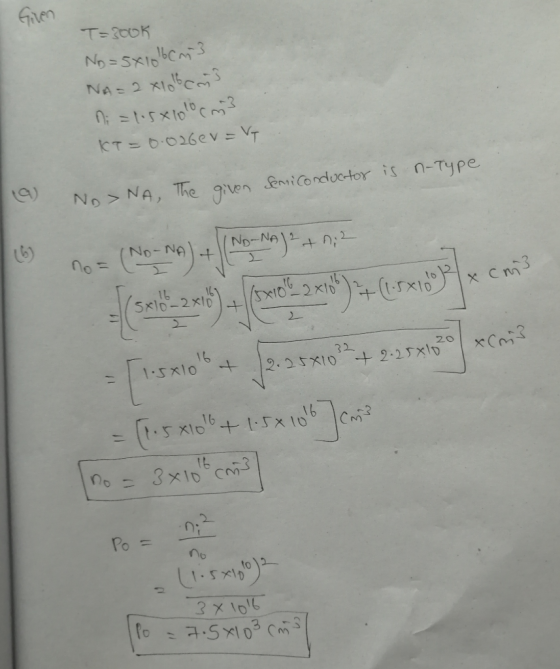
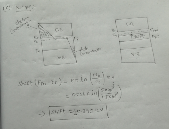
Problem 1 (25 points) Si at T = 300K contains donor impurity atoms at a density of 5x 10'6cm and ...
1. a. Find the main error in each of the band diagrams shown below. For all...
 1. a. Find the main error in each of the band diagrams shown below. For all of the band diagrams Ny 1019/cm3, Ne- 1019/cm3, ni = 3 x 10⁸/cm". E,-1.25 eV, T = 300 K. Ef Ef EFi Main error: Main error: Main error: Main error: Consider a semiconductor sample with the following characteristics: EG 1.25 eV, T 300 K, Nd 5 x 101*/cm3, Na 1014/cm3, N.-1019/cm3, N.-1019/cm3, ni-3 × 10⁸/cm3. Assume complete ionization b. Find the equilibrium electron and...
1. Define the majority carrier concentration in an n-type Si semiconductor in terms of the conduction...
 1. Define the majority carrier concentration in an n-type Si semiconductor in terms of the conduction band edge energy Ec and the Fermi energy Ep 2 marks Find an expression for Ec - Ep, i.e, the difference between the conduction band edge energy and the Fermi energy in terms of the donor concentration Np. 4 marks Determine the concentration of donor impurity atoms that must be added to silicon that Ec Ef = 0.2 eV So 4 marks
Define the majority carrier concentration in an n-type Si semiconductor in terms of the conduction band...
 Define the majority carrier concentration in an n-type Si semiconductor in terms of the conduction band edge energy E, and the Fermi energy E. 1. 2 marks Find an expression for Ee -Ef, i.e, the difference between the conduction band edge energy and the Fermi energy in terms of the donor concentration ND. 4 marks Determine the concentration of donor impurity atoms that must be added to silicon so that Ec- E0.2 eV. 3 marks
6. A silicon wafer is doped with donor atoms, N-5x0 cm(bonus question) (a) Determine (Ec-EF), (EF...
 6. A silicon wafer is doped with donor atoms, N-5x0 cm(bonus question) (a) Determine (Ec-EF), (EF-Ev), (Ep-E) at 300 K. Assume all the donor atoms are ionized. (b) Plot the position of Fermi level (EF) in the bandgap as a function of temperature for 300 Ts700 K. In this temperature range, it can be assumed that all the donor atoms are ionized. (c) Plot the position of Fermi level (Er) in the bandgap as acceptor atoms are added (N.- 104,...
Silicon at at T-300 K contains acceptor atoms at a concentration of Na-5x10A15 cmA-3. Donor atoms are added forming an n type compensated(counter doped) semiconductor such that the fermi level is 0.2...
 Silicon at at T-300 K contains acceptor atoms at a concentration of Na-5x10A15 cmA-3. Donor atoms are added forming an n type compensated(counter doped) semiconductor such that the fermi level is 0.215 eV below the conduction band edge 4. a. What concentration of donor atoms were added. b. What were the concentration of holes and electrons before the silicon was counterdoped c. What are the electron and hole concentrations after the silicon was counter doped.
Silicon at at T-300 K...
Silicon at at T-300 K contains acceptor atoms at a concentration of Na-5x10A15 cmA-3. Donor atoms are added forming an n type compensated(counter doped) semiconductor such that the fermi level is 0.215 eV below the conduction band edge 4. a. What concentration of donor atoms were added. b. What were the concentration of holes and electrons before the silicon was counterdoped c. What are the electron and hole concentrations after the silicon was counter doped.
Silicon at at T-300 K...
Silicon at at T-300 K contains acceptor atoms at a concentration of Na-5x10A15 cmA-3. Donor atoms are added forming an n type compensated(counter doped) semiconductor such that the fermi level is 0.2...
 Silicon at at T-300 K contains acceptor atoms at a concentration of Na-5x10A15 cmA-3. Donor atoms are added forming an n type compensated(counter doped) semiconductor such that the fermi level is 0.215 eV below the conduction band edge 4. a. What concentration of donor atoms were added. b. What were the concentration of holes and electrons before the silicon was counterdoped c. What are the electron and hole concentrations after the silicon was counter doped.
Silicon at at T-300 K...
Silicon at at T-300 K contains acceptor atoms at a concentration of Na-5x10A15 cmA-3. Donor atoms are added forming an n type compensated(counter doped) semiconductor such that the fermi level is 0.215 eV below the conduction band edge 4. a. What concentration of donor atoms were added. b. What were the concentration of holes and electrons before the silicon was counterdoped c. What are the electron and hole concentrations after the silicon was counter doped.
Silicon at at T-300 K...
EENG 245 Physical electronics HW 1 1) The NaCl crystal is cubic, and can be described...
 EENG 245 Physical electronics HW 1 1) The NaCl crystal is cubic, and can be described as follows. Na atoms sit at the corners and faces of a cube, and Cl atoms sit in between two Na atoms. This means that a Clatom is found half-way along each of the cube edges, and there is a Cl in the center of the cube. (We could also have described the lattice by interchanging Na and Cl in the description above.) Another...
P3. (a) Determine the position of the Fermi level with respect to the intrinsic Fermi level in silicon at T =...
 P3. (a) Determine the position of the Fermi level with respect to the intrinsic Fermi level in silicon at T = 300'K that is doped with phosphors atoms at a concentration of 1015 cm. (b) Repeat (a) if the silicon is doped with boron atoms at a concentration of 10'5 cm3. (c) Calculate the electron concentration in the silicon for parts (a) and (b) P1. For the Boltzmann approximation to be valid for a semiconductor, the Fermi level must be...
For a Si p-n junction with p-type doping of 1 x 10^16/cm3 and n-type doping of...
For a Si p-n junction with p-type doping of 1 x 10^16/cm3 and n-type doping of 1 x 10^19/cm3, calculate the built-in potential Vb at 300K, dark, thermal equilibrium condition. Please show the equations and parameters used in the calculation and the value of Ec-Ef, Ef-Ev, and Vb. Please draw a band structure similar to the one in lecture 5 slide 6 based on your results, please also label Ec, Ev, Vb, and Ef in the drawing.
Electronic ECE
 P and N type semiconductors are formed with an acceptor and donor concentration of 1×1017 cm-3 and 1×1016 cm-3 , respectively,
intrinsic carrier concentration is 1×1010 cm-3 and relative permittivity (єs
) is 12є0 @ 300K.
Given, permittivity of free space (є0
) 8.85 × 10⁻¹² Farad/meter, KT @ 300K 0.0259 eV, q = 1.602 × 10⁻¹⁹ coulombs2. Majority and Minority Electron density (in cm-3
) & Hole density (in cm-3
) under equilibrium B. Draw the following profiles @ 300K 3....
P and N type semiconductors are formed with an acceptor and donor concentration of 1×1017 cm-3 and 1×1016 cm-3 , respectively,
intrinsic carrier concentration is 1×1010 cm-3 and relative permittivity (єs
) is 12є0 @ 300K.
Given, permittivity of free space (є0
) 8.85 × 10⁻¹² Farad/meter, KT @ 300K 0.0259 eV, q = 1.602 × 10⁻¹⁹ coulombs2. Majority and Minority Electron density (in cm-3
) & Hole density (in cm-3
) under equilibrium B. Draw the following profiles @ 300K 3....
 1. a. Find the main error in each of the band diagrams shown below. For all of the band diagrams Ny 1019/cm3, Ne- 1019/cm3, ni = 3 x 10⁸/cm". E,-1.25 eV, T = 300 K. Ef Ef EFi Main error: Main error: Main error: Main error: Consider a semiconductor sample with the following characteristics: EG 1.25 eV, T 300 K, Nd 5 x 101*/cm3, Na 1014/cm3, N.-1019/cm3, N.-1019/cm3, ni-3 × 10⁸/cm3. Assume complete ionization b. Find the equilibrium electron and...
 1. Define the majority carrier concentration in an n-type Si semiconductor in terms of the conduction band edge energy Ec and the Fermi energy Ep 2 marks Find an expression for Ec - Ep, i.e, the difference between the conduction band edge energy and the Fermi energy in terms of the donor concentration Np. 4 marks Determine the concentration of donor impurity atoms that must be added to silicon that Ec Ef = 0.2 eV So 4 marks
 Define the majority carrier concentration in an n-type Si semiconductor in terms of the conduction band edge energy E, and the Fermi energy E. 1. 2 marks Find an expression for Ee -Ef, i.e, the difference between the conduction band edge energy and the Fermi energy in terms of the donor concentration ND. 4 marks Determine the concentration of donor impurity atoms that must be added to silicon so that Ec- E0.2 eV. 3 marks
 6. A silicon wafer is doped with donor atoms, N-5x0 cm(bonus question) (a) Determine (Ec-EF), (EF-Ev), (Ep-E) at 300 K. Assume all the donor atoms are ionized. (b) Plot the position of Fermi level (EF) in the bandgap as a function of temperature for 300 Ts700 K. In this temperature range, it can be assumed that all the donor atoms are ionized. (c) Plot the position of Fermi level (Er) in the bandgap as acceptor atoms are added (N.- 104,...
 Silicon at at T-300 K contains acceptor atoms at a concentration of Na-5x10A15 cmA-3. Donor atoms are added forming an n type compensated(counter doped) semiconductor such that the fermi level is 0.215 eV below the conduction band edge 4. a. What concentration of donor atoms were added. b. What were the concentration of holes and electrons before the silicon was counterdoped c. What are the electron and hole concentrations after the silicon was counter doped.
Silicon at at T-300 K...
Silicon at at T-300 K contains acceptor atoms at a concentration of Na-5x10A15 cmA-3. Donor atoms are added forming an n type compensated(counter doped) semiconductor such that the fermi level is 0.215 eV below the conduction band edge 4. a. What concentration of donor atoms were added. b. What were the concentration of holes and electrons before the silicon was counterdoped c. What are the electron and hole concentrations after the silicon was counter doped.
Silicon at at T-300 K...
 Silicon at at T-300 K contains acceptor atoms at a concentration of Na-5x10A15 cmA-3. Donor atoms are added forming an n type compensated(counter doped) semiconductor such that the fermi level is 0.215 eV below the conduction band edge 4. a. What concentration of donor atoms were added. b. What were the concentration of holes and electrons before the silicon was counterdoped c. What are the electron and hole concentrations after the silicon was counter doped.
Silicon at at T-300 K...
Silicon at at T-300 K contains acceptor atoms at a concentration of Na-5x10A15 cmA-3. Donor atoms are added forming an n type compensated(counter doped) semiconductor such that the fermi level is 0.215 eV below the conduction band edge 4. a. What concentration of donor atoms were added. b. What were the concentration of holes and electrons before the silicon was counterdoped c. What are the electron and hole concentrations after the silicon was counter doped.
Silicon at at T-300 K...
 EENG 245 Physical electronics HW 1 1) The NaCl crystal is cubic, and can be described as follows. Na atoms sit at the corners and faces of a cube, and Cl atoms sit in between two Na atoms. This means that a Clatom is found half-way along each of the cube edges, and there is a Cl in the center of the cube. (We could also have described the lattice by interchanging Na and Cl in the description above.) Another...
 P3. (a) Determine the position of the Fermi level with respect to the intrinsic Fermi level in silicon at T = 300'K that is doped with phosphors atoms at a concentration of 1015 cm. (b) Repeat (a) if the silicon is doped with boron atoms at a concentration of 10'5 cm3. (c) Calculate the electron concentration in the silicon for parts (a) and (b) P1. For the Boltzmann approximation to be valid for a semiconductor, the Fermi level must be...
Most questions answered within 3 hours.
-
Where is the error in this code sequence?
String s1 = "Hello";
String s2 = "ello";...
asked 11 months ago -
Financial data for Joel de Paris, Inc., for last year
follow:
Joel de Paris, Inc.
Balance...
asked 11 months ago -
Consider this reaction:
Al2(SO4)3 (aq)+ BaCl3
(aq) Al2Cl6 (aq)- +
3BaSO4(s) . What is the...
asked 11 months ago -
Suppose that Savneet is considering increasing her
recent random sample from 20 car rentals to 40...
asked 11 months ago -
Trucks arrive at an unloading terminal at an average rate of 120
per hour.
Trucks arrive...
asked 11 months ago -
Why are methanol and ethanol completely soluble in water while
octanol is not very little soluble....
asked 11 months ago -
A facilities manager at a university reads in a research report
that the mean amount of...
asked 11 months ago -
When the CuSO4 is rehydrated by adding water to the anhydrous
compound, is this an endothermic...
asked 11 months ago -
A ray of sunlight is passing from diamond into crown glass; the
angle of incidence is...
asked 11 months ago -
A block of mass 0.249 kg is placed on top of a light, vertical
spring of...
asked 11 months ago -
how do the kidneys compensate in the presences of acidosis
a) trigger hyperventilate
b) reserve acid...
asked 11 months ago -
Question 501 pts
The rental rate of capital to the firm increases. Which of the
following...
asked 11 months ago