
Homework Answers
Summary - it is basic problem so I have shown step by step
solution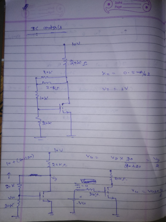
Add Answer to:
#3. (35 p) Find the voltage gain input and ouipul resistance of the ampli ifier circuit below, wh...
3. Design a n-channel JFET C-S amplifier circuit for the following specifications Voltage Gain input resistance...
 3. Design a n-channel JFET C-S amplifier circuit for the following specifications Voltage Gain input resistance Ri-100kΩ Load resistanceR2k2 Given supply voltage VDD 20V Αν--10 Rss is fully bypassed The input source resistance Rs 02, Ipss-8mA and Vp4V Assume RD and R1 but must find R2 and RSS using the given specifications. Find the DC Operating Points values (VGs, ID and VDs) Draw the actual circuit and its ac equivalent circuit
Find the expression for voltage gain Avj, input resistance Rif and output resistance Roffor the circuit...
 Find the expression for voltage gain Avj, input
resistance Rif and output resistance Roffor
the circuit shown in Fig. for Q. 5(b)
(b) Find the expression for voltage gain Av, input resistance Rif and output resistance Rof for the circuit shown in Fig. for Q. 5(b) A DD RD
Find the expression for voltage gain Avj, input
resistance Rif and output resistance Roffor
the circuit shown in Fig. for Q. 5(b)
(b) Find the expression for voltage gain Av, input resistance Rif and output resistance Rof for the circuit shown in Fig. for Q. 5(b) A DD RD
vo 3. (30%) For the circuit below: a) Find an expression for the gain , b)...
 vo 3. (30%) For the circuit below: a) Find an expression for the gain , b) The output impedance including vi the effect of ro, c) The maximum voltage (DC+AC value) at the output in large signal analysis. VDD RD Vị BONUS (10%): The gain of the circuit including the effect of ro
Small-Signal Mid- Band Voltage Gain (Range) Transistors Amplifier Confiaurations +2) to (+5 P-JFET Common Gate By referring to a specific transistor datasheet, design a single stage amplifier circuit...
 Small-Signal Mid- Band Voltage Gain (Range) Transistors Amplifier Confiaurations +2) to (+5 P-JFET Common Gate By referring to a specific transistor datasheet, design a single stage amplifier circuit with the following specifications. Include in your design, (i) the amplifier circuit, (ii) DC & AC equivalent circuits, (ii) DC & AC analysis and (iv) frequency response. State your assumptions, if any.
Small-Signal Mid- Band Voltage Gain (Range) Transistors Amplifier Confiaurations +2) to (+5 P-JFET Common Gate By referring to a specific...
Small-Signal Mid- Band Voltage Gain (Range) Transistors Amplifier Confiaurations +2) to (+5 P-JFET Common Gate By referring to a specific transistor datasheet, design a single stage amplifier circuit with the following specifications. Include in your design, (i) the amplifier circuit, (ii) DC & AC equivalent circuits, (ii) DC & AC analysis and (iv) frequency response. State your assumptions, if any.
Small-Signal Mid- Band Voltage Gain (Range) Transistors Amplifier Confiaurations +2) to (+5 P-JFET Common Gate By referring to a specific...
Please show steps & explain. WILL RATE!!! 7.133 For the circuit below, find the input resistance...
 Please show steps &
explain. WILL RATE!!!
7.133 For the circuit below, find the input resistance Rin and the voltage gain v./Vsig. Assume that the source provides a small signal Vsig and that ß = 100. 0.5 mA tovo § 5 KN 100 kN 3 Rsig = 50 12 U18
Please show steps &
explain. WILL RATE!!!
7.133 For the circuit below, find the input resistance Rin and the voltage gain v./Vsig. Assume that the source provides a small signal Vsig and that ß = 100. 0.5 mA tovo § 5 KN 100 kN 3 Rsig = 50 12 U18
The depicted circuit represents a CE gain stage. Find a value for the dc input resistance ri (in ...
 The depicted circuit represents a CE gain stage. Find a value for the dc input resistance ri (in Ω) of this equivalent circuit. BJT Transistor Rs ο Ιβ=150 +VA 60 V Cu Vs nVT 30 mV
The depicted circuit represents a CE gain stage. Find a value for the dc input resistance ri (in Ω) of this equivalent circuit. BJT Transistor Rs ο Ιβ=150 +VA 60 V Cu Vs nVT 30 mV
The depicted circuit represents a CE gain stage. Find a value for the dc input resistance ri (in Ω) of this equivalent circuit. BJT Transistor Rs ο Ιβ=150 +VA 60 V Cu Vs nVT 30 mV
a) Calculate the theoretical Voltage Gain, Input resistance, and Output resistance for the circuit used in...
 a) Calculate the theoretical Voltage Gain, Input resistance,
and Output resistance for the circuit used in this lab. Assume
Beta= 200 and that the signal generator has an output resistance of
50ohm
find Av? Rin? Rout?
vec 20.00 XSC1 (RB 470kg Tektronix C2 HE 100F 1 2N4124 CA M - 100F RE 32.2ko RL 1ko w
a) Calculate the theoretical Voltage Gain, Input resistance,
and Output resistance for the circuit used in this lab. Assume
Beta= 200 and that the signal generator has an output resistance of
50ohm
find Av? Rin? Rout?
vec 20.00 XSC1 (RB 470kg Tektronix C2 HE 100F 1 2N4124 CA M - 100F RE 32.2ko RL 1ko w
C- Amplifier: Consider figure 3. This circuit uses the JFET to amplify the input signal voltage F...
 C- Amplifier: Consider figure 3. This circuit uses the JFET to amplify the input signal voltage First the dc operation must be set. Use equation 1 and your previous data to calculate the value of Vas required to give I-0.5 mA. Determine the source resistance Rs needed to set this bias. Set up the circuit of figure 3 with your calculated value of Rs. Measure Vo and Vs to determine if your operating conditions are correct. Apply an input voltage...
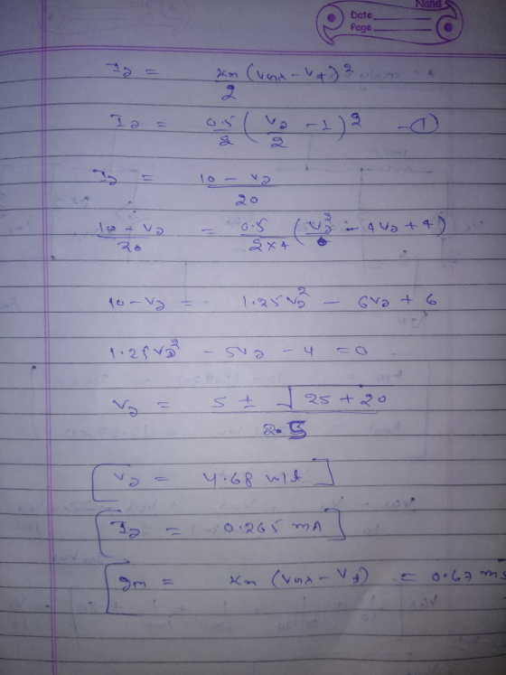
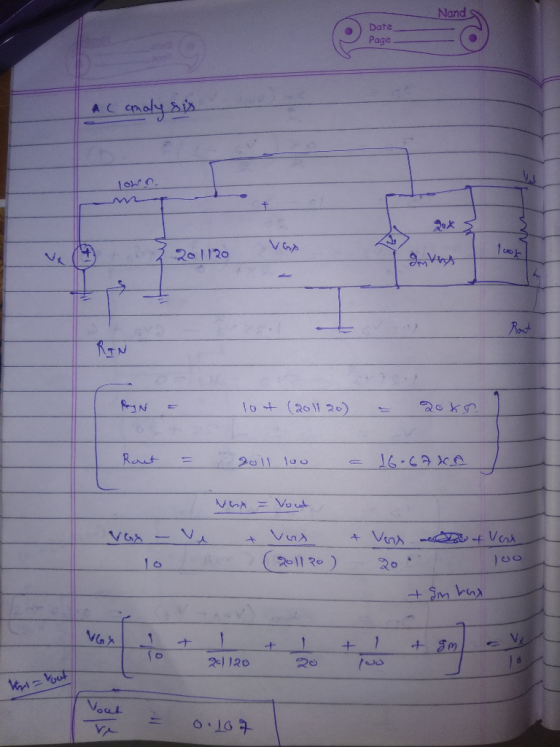
Analog Integrated Circuits Exercise 3 1. Express (a) voltage gain, (b) input resistance, and (c) output...
 Analog Integrated Circuits Exercise 3 1. Express (a) voltage gain, (b) input resistance, and (c) output resistance of the following circut. RD B1 M1 M2 B2 Vss
Obtain voltage gain, input resistance and output resistance from the following circuits. (However,VA = ∞ and...
 Obtain voltage gain, input resistance and output resistance from
the following circuits. (However,VA = ∞ and the internal parameters
of
can be displayed in
, and all transistors operate in the Active area (or at least Soft
saturation)
ON "A, 8m, B VCC Q4 Vout V in Q w R1 Q2
Obtain voltage gain, input resistance and output resistance from
the following circuits. (However,VA = ∞ and the internal parameters
of
can be displayed in
, and all transistors operate in the Active area (or at least Soft
saturation)
ON "A, 8m, B VCC Q4 Vout V in Q w R1 Q2
 3. Design a n-channel JFET C-S amplifier circuit for the following specifications Voltage Gain input resistance Ri-100kΩ Load resistanceR2k2 Given supply voltage VDD 20V Αν--10 Rss is fully bypassed The input source resistance Rs 02, Ipss-8mA and Vp4V Assume RD and R1 but must find R2 and RSS using the given specifications. Find the DC Operating Points values (VGs, ID and VDs) Draw the actual circuit and its ac equivalent circuit
 Find the expression for voltage gain Avj, input
resistance Rif and output resistance Roffor
the circuit shown in Fig. for Q. 5(b)
(b) Find the expression for voltage gain Av, input resistance Rif and output resistance Rof for the circuit shown in Fig. for Q. 5(b) A DD RD
Find the expression for voltage gain Avj, input
resistance Rif and output resistance Roffor
the circuit shown in Fig. for Q. 5(b)
(b) Find the expression for voltage gain Av, input resistance Rif and output resistance Rof for the circuit shown in Fig. for Q. 5(b) A DD RD
 vo 3. (30%) For the circuit below: a) Find an expression for the gain , b) The output impedance including vi the effect of ro, c) The maximum voltage (DC+AC value) at the output in large signal analysis. VDD RD Vị BONUS (10%): The gain of the circuit including the effect of ro
 Small-Signal Mid- Band Voltage Gain (Range) Transistors Amplifier Confiaurations +2) to (+5 P-JFET Common Gate By referring to a specific transistor datasheet, design a single stage amplifier circuit with the following specifications. Include in your design, (i) the amplifier circuit, (ii) DC & AC equivalent circuits, (ii) DC & AC analysis and (iv) frequency response. State your assumptions, if any.
Small-Signal Mid- Band Voltage Gain (Range) Transistors Amplifier Confiaurations +2) to (+5 P-JFET Common Gate By referring to a specific...
Small-Signal Mid- Band Voltage Gain (Range) Transistors Amplifier Confiaurations +2) to (+5 P-JFET Common Gate By referring to a specific transistor datasheet, design a single stage amplifier circuit with the following specifications. Include in your design, (i) the amplifier circuit, (ii) DC & AC equivalent circuits, (ii) DC & AC analysis and (iv) frequency response. State your assumptions, if any.
Small-Signal Mid- Band Voltage Gain (Range) Transistors Amplifier Confiaurations +2) to (+5 P-JFET Common Gate By referring to a specific...
 Please show steps &
explain. WILL RATE!!!
7.133 For the circuit below, find the input resistance Rin and the voltage gain v./Vsig. Assume that the source provides a small signal Vsig and that ß = 100. 0.5 mA tovo § 5 KN 100 kN 3 Rsig = 50 12 U18
Please show steps &
explain. WILL RATE!!!
7.133 For the circuit below, find the input resistance Rin and the voltage gain v./Vsig. Assume that the source provides a small signal Vsig and that ß = 100. 0.5 mA tovo § 5 KN 100 kN 3 Rsig = 50 12 U18
 The depicted circuit represents a CE gain stage. Find a value for the dc input resistance ri (in Ω) of this equivalent circuit. BJT Transistor Rs ο Ιβ=150 +VA 60 V Cu Vs nVT 30 mV
The depicted circuit represents a CE gain stage. Find a value for the dc input resistance ri (in Ω) of this equivalent circuit. BJT Transistor Rs ο Ιβ=150 +VA 60 V Cu Vs nVT 30 mV
The depicted circuit represents a CE gain stage. Find a value for the dc input resistance ri (in Ω) of this equivalent circuit. BJT Transistor Rs ο Ιβ=150 +VA 60 V Cu Vs nVT 30 mV
 a) Calculate the theoretical Voltage Gain, Input resistance,
and Output resistance for the circuit used in this lab. Assume
Beta= 200 and that the signal generator has an output resistance of
50ohm
find Av? Rin? Rout?
vec 20.00 XSC1 (RB 470kg Tektronix C2 HE 100F 1 2N4124 CA M - 100F RE 32.2ko RL 1ko w
a) Calculate the theoretical Voltage Gain, Input resistance,
and Output resistance for the circuit used in this lab. Assume
Beta= 200 and that the signal generator has an output resistance of
50ohm
find Av? Rin? Rout?
vec 20.00 XSC1 (RB 470kg Tektronix C2 HE 100F 1 2N4124 CA M - 100F RE 32.2ko RL 1ko w
 C- Amplifier: Consider figure 3. This circuit uses the JFET to amplify the input signal voltage First the dc operation must be set. Use equation 1 and your previous data to calculate the value of Vas required to give I-0.5 mA. Determine the source resistance Rs needed to set this bias. Set up the circuit of figure 3 with your calculated value of Rs. Measure Vo and Vs to determine if your operating conditions are correct. Apply an input voltage...
 Analog Integrated Circuits Exercise 3 1. Express (a) voltage gain, (b) input resistance, and (c) output resistance of the following circut. RD B1 M1 M2 B2 Vss
 Obtain voltage gain, input resistance and output resistance from
the following circuits. (However,VA = ∞ and the internal parameters
of
can be displayed in
, and all transistors operate in the Active area (or at least Soft
saturation)
ON "A, 8m, B VCC Q4 Vout V in Q w R1 Q2
Obtain voltage gain, input resistance and output resistance from
the following circuits. (However,VA = ∞ and the internal parameters
of
can be displayed in
, and all transistors operate in the Active area (or at least Soft
saturation)
ON "A, 8m, B VCC Q4 Vout V in Q w R1 Q2
Most questions answered within 3 hours.
-
Where is the error in this code sequence?
String s1 = "Hello";
String s2 = "ello";...
asked 11 months ago -
Financial data for Joel de Paris, Inc., for last year
follow:
Joel de Paris, Inc.
Balance...
asked 11 months ago -
Consider this reaction:
Al2(SO4)3 (aq)+ BaCl3
(aq) Al2Cl6 (aq)- +
3BaSO4(s) . What is the...
asked 11 months ago -
Suppose that Savneet is considering increasing her
recent random sample from 20 car rentals to 40...
asked 11 months ago -
Trucks arrive at an unloading terminal at an average rate of 120
per hour.
Trucks arrive...
asked 11 months ago -
Why are methanol and ethanol completely soluble in water while
octanol is not very little soluble....
asked 11 months ago -
A facilities manager at a university reads in a research report
that the mean amount of...
asked 11 months ago -
When the CuSO4 is rehydrated by adding water to the anhydrous
compound, is this an endothermic...
asked 11 months ago -
A ray of sunlight is passing from diamond into crown glass; the
angle of incidence is...
asked 11 months ago -
A block of mass 0.249 kg is placed on top of a light, vertical
spring of...
asked 11 months ago -
how do the kidneys compensate in the presences of acidosis
a) trigger hyperventilate
b) reserve acid...
asked 11 months ago -
Question 501 pts
The rental rate of capital to the firm increases. Which of the
following...
asked 11 months ago