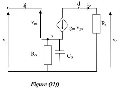
Figure Q1f) shows the ac equivalent circuit of a common-source amplifier where Rt is the ac load.
f) Figure Q1f) shows the ac equivalent circuit of a common-source amplifier where Rt is the ac load. The low-frequency roll-off is to be set by the capacitor Cs. Design the amplifier to have a low-frequency roll-off, fL = 100 Hz. You may assume that Rs is much greater than the impedance of Cs at the frequency of 100 Hz. (gm = 1 mA/V)
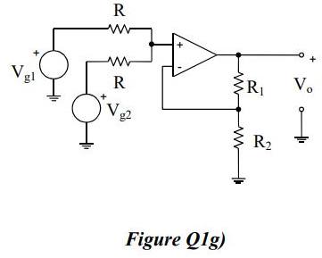
g) The op-amp in Figure Q1g) is ideal. For the condition R1 = R2, show that the output voltage, V0 is given by, V0 = Vg1 + Vg2.
How would you modify the circuit to obtain a gain of 10?
State all assumptions used in your analysis.
Homework Answers


Add Answer to:
Figure Q1f) shows the ac equivalent circuit of a common-source amplifier where Rt is the ac load.
f) Figure Qlf) shows the ac equivalent circuit of a common-source amplifier where have a low-frequeney rol-off C assume that Rs is much greater than the impedance of Cs at the frequency of 100 Re is...
 f) Figure Qlf) shows the ac equivalent circuit of a common-source amplifier where have a low-frequeney rol-off C assume that Rs is much greater than the impedance of Cs at the frequency of 100 Re is the ac load. The low-frequency roll-off is to be set by the capacitor Cs. Design the amplifier to have a low-frequency roll-off, 100 Hz. You may Rt gs gm Vgs V. Rs Cs Figure QiD
f) Figure Qlf) shows the ac equivalent circuit of...
f) Figure Qlf) shows the ac equivalent circuit of a common-source amplifier where have a low-frequeney rol-off C assume that Rs is much greater than the impedance of Cs at the frequency of 100 Re is the ac load. The low-frequency roll-off is to be set by the capacitor Cs. Design the amplifier to have a low-frequency roll-off, 100 Hz. You may Rt gs gm Vgs V. Rs Cs Figure QiD
f) Figure Qlf) shows the ac equivalent circuit of...
(a) A voltage divider bypassed common-source (CS) FET amplifier biasing circuit with load R, is commonly...
 (a) A voltage divider bypassed common-source (CS) FET amplifier biasing circuit with load R, is commonly used in electronic circuit. (1) Design the circuit of a voltage divider bypassed common-source FET amplifier biasing circuit with load Ru. [4 marks) (ii) By referring to Q4(a)(i), design a bypassed common-source FET amplifier with biasing voltage-divider to meet the given specifications below: Supply voltage, Vcc = 12 V; Voltage gain, Ay = -10; Output load Ru = 10 kV2; input impedance Zi =...
Please solve this Question Figure Q4 shows a common-source amplifier. Construct the ac equivalent circuit, then apply M...
 Please solve this Question
Figure Q4 shows a common-source amplifier. Construct the ac equivalent circuit, then apply Miller's Theorem and hence show that the voltage gain is given as: where J-is the voltage gain bandwidth. R, = RD //RL and C-C,, + (I + g.Rjcgd」 State clearly any approximations or assumptions used in your analysis. The parameters above are defined as follows: gm is the transistor transconductance, Ce and Cet are the internal capacitances between the gate/source and gate/drain respectively...
Please solve this Question
Figure Q4 shows a common-source amplifier. Construct the ac equivalent circuit, then apply Miller's Theorem and hence show that the voltage gain is given as: where J-is the voltage gain bandwidth. R, = RD //RL and C-C,, + (I + g.Rjcgd」 State clearly any approximations or assumptions used in your analysis. The parameters above are defined as follows: gm is the transistor transconductance, Ce and Cet are the internal capacitances between the gate/source and gate/drain respectively...
Figure 2 shows a multiple op-amp networks combined to produce a gain amplifier circuit. For the...
 Figure 2 shows a multiple op-amp networks combined to produce a gain amplifier circuit. For the given circuit: (i) Name all the type of op-amp circuits shown by Op-Amp 1 until Op-Amp 5. (ii) Calculate the output of each Op-Amp 1 until Op-Amp 4. Assume Vin = 10mV (iii) Determine the output voltage at the last Op-Amp 5. From this value, calculate the gain produced by this Op-Amp network in overall, by using Av=Vos / Vin equation. [10 Marks] CO3,...
1. The following circuit shows a discrete common source MOSFET amplifier. The MOSFTE is n-channel MOSFET...
 1. The following circuit shows a discrete common source MOSFET amplifier. The MOSFTE is n-channel MOSFET and early voltage (Va) is c. The transconductance of the amplifier (ga) is 3 mA/V The frequency responses of the amplifier are as follows i) The three low break frequencies f 3Hz (caused by C).fiz-S0Hz (caused by Cs). fs-10Hz (caused by Ca) ii) High 3 dB frequency. f-30kHz ii) The MOSFET unity gain frequency fr-100 MHz (a) Draw small signal equivalent circuit of the...
A common source amplifier circuit based on a single n-channel MOSFET is shown in Figure 4b. Assume that the transconductance gm-60 mS (equivalent to mA/ V) and drain source resistance, os,...
 A common source amplifier circuit based on a single n-channel MOSFET is shown in Figure 4b. Assume that the transconductance gm-60 mS (equivalent to mA/ V) and drain source resistance, os, is so large it may be neglected. 0) Calculate the open circuit voltage gain Av Yout/ Vis. i) The amplifier has a load of 10 k2. Determine the current gain Va. = 12 V 150k 4k3 Vout Vin 200k GND = 0 V Figure 4b a) State the name...
The NMOS transistor in the CS amplifier circuit of the figure is biased to have gn=4mA/V....
 The NMOS transistor in the CS amplifier circuit of the figure is biased to have gn=4mA/V. a)Find Am, fpi, fp2, fp3, and fl. (Assume the largest pole value as fl) b)Assume that the same amplifier is biased to have gm=lmA/V, 19=100k 2, Cgs=1pF, Cgd=0.2pF, Find Am and fu. You can use approximation methods. c) Draw the overall frequency response. VPD 47 ΜΩ 4.7 k12 w OV 100 k12 0.1 uF MH 10 k12 0.01 uF +1 10 ΜΩ 2 ΚΩ...
Circuit Analysis Zo Is Zi ALi If FIGURE Q3(b) negative feedback network (b) Figure Q3(b) shows...
 Circuit Analysis
Zo Is Zi ALi If FIGURE Q3(b) negative feedback network (b) Figure Q3(b) shows an amplifier with a Given Zof 100 kQ, Zo = 10 kQ and A 50 State the feedback topology and the amplifier type (i) (2 marks) (ii) Calculate the gain without feedback, A and the feedback factor, B. (6 marks) (iii) If the low cutoff frequency of the amplifier with feedback network (fL) is 300 Hz, calculate the low cutoff frequency (fi) if the...
Circuit Analysis
Zo Is Zi ALi If FIGURE Q3(b) negative feedback network (b) Figure Q3(b) shows an amplifier with a Given Zof 100 kQ, Zo = 10 kQ and A 50 State the feedback topology and the amplifier type (i) (2 marks) (ii) Calculate the gain without feedback, A and the feedback factor, B. (6 marks) (iii) If the low cutoff frequency of the amplifier with feedback network (fL) is 300 Hz, calculate the low cutoff frequency (fi) if the...
C- Amplifier: Consider figure 3. This circuit uses the JFET to amplify the input signal voltage F...
 C- Amplifier: Consider figure 3. This circuit uses the JFET to amplify the input signal voltage First the dc operation must be set. Use equation 1 and your previous data to calculate the value of Vas required to give I-0.5 mA. Determine the source resistance Rs needed to set this bias. Set up the circuit of figure 3 with your calculated value of Rs. Measure Vo and Vs to determine if your operating conditions are correct. Apply an input voltage...
Figure 2 shows a feedback amplifier circuit. Rs is the source resistor and R, is the...
 Figure 2 shows a feedback amplifier circuit. Rs is the source resistor and R, is the load resistor RS Vs VI RL OPAMP R2 R1 RM R3 R4 Step 1: open-loop and closed-loop circuits identification 1.1 Identify the source, the load, and the closed-loop amplifier 1.2 Identify the open-loop amplifier (**A" eireuit) and the feedback network (B" eircuit) in the closed-loop amplifier 1.3 Identify the connection type between the "A" circuit and the "B" circuit at both the input and...
 f) Figure Qlf) shows the ac equivalent circuit of a common-source amplifier where have a low-frequeney rol-off C assume that Rs is much greater than the impedance of Cs at the frequency of 100 Re is the ac load. The low-frequency roll-off is to be set by the capacitor Cs. Design the amplifier to have a low-frequency roll-off, 100 Hz. You may Rt gs gm Vgs V. Rs Cs Figure QiD
f) Figure Qlf) shows the ac equivalent circuit of...
f) Figure Qlf) shows the ac equivalent circuit of a common-source amplifier where have a low-frequeney rol-off C assume that Rs is much greater than the impedance of Cs at the frequency of 100 Re is the ac load. The low-frequency roll-off is to be set by the capacitor Cs. Design the amplifier to have a low-frequency roll-off, 100 Hz. You may Rt gs gm Vgs V. Rs Cs Figure QiD
f) Figure Qlf) shows the ac equivalent circuit of...
 (a) A voltage divider bypassed common-source (CS) FET amplifier biasing circuit with load R, is commonly used in electronic circuit. (1) Design the circuit of a voltage divider bypassed common-source FET amplifier biasing circuit with load Ru. [4 marks) (ii) By referring to Q4(a)(i), design a bypassed common-source FET amplifier with biasing voltage-divider to meet the given specifications below: Supply voltage, Vcc = 12 V; Voltage gain, Ay = -10; Output load Ru = 10 kV2; input impedance Zi =...
 Please solve this Question
Figure Q4 shows a common-source amplifier. Construct the ac equivalent circuit, then apply Miller's Theorem and hence show that the voltage gain is given as: where J-is the voltage gain bandwidth. R, = RD //RL and C-C,, + (I + g.Rjcgd」 State clearly any approximations or assumptions used in your analysis. The parameters above are defined as follows: gm is the transistor transconductance, Ce and Cet are the internal capacitances between the gate/source and gate/drain respectively...
Please solve this Question
Figure Q4 shows a common-source amplifier. Construct the ac equivalent circuit, then apply Miller's Theorem and hence show that the voltage gain is given as: where J-is the voltage gain bandwidth. R, = RD //RL and C-C,, + (I + g.Rjcgd」 State clearly any approximations or assumptions used in your analysis. The parameters above are defined as follows: gm is the transistor transconductance, Ce and Cet are the internal capacitances between the gate/source and gate/drain respectively...
 Figure 2 shows a multiple op-amp networks combined to produce a gain amplifier circuit. For the given circuit: (i) Name all the type of op-amp circuits shown by Op-Amp 1 until Op-Amp 5. (ii) Calculate the output of each Op-Amp 1 until Op-Amp 4. Assume Vin = 10mV (iii) Determine the output voltage at the last Op-Amp 5. From this value, calculate the gain produced by this Op-Amp network in overall, by using Av=Vos / Vin equation. [10 Marks] CO3,...
 1. The following circuit shows a discrete common source MOSFET amplifier. The MOSFTE is n-channel MOSFET and early voltage (Va) is c. The transconductance of the amplifier (ga) is 3 mA/V The frequency responses of the amplifier are as follows i) The three low break frequencies f 3Hz (caused by C).fiz-S0Hz (caused by Cs). fs-10Hz (caused by Ca) ii) High 3 dB frequency. f-30kHz ii) The MOSFET unity gain frequency fr-100 MHz (a) Draw small signal equivalent circuit of the...
 A common source amplifier circuit based on a single n-channel MOSFET is shown in Figure 4b. Assume that the transconductance gm-60 mS (equivalent to mA/ V) and drain source resistance, os, is so large it may be neglected. 0) Calculate the open circuit voltage gain Av Yout/ Vis. i) The amplifier has a load of 10 k2. Determine the current gain Va. = 12 V 150k 4k3 Vout Vin 200k GND = 0 V Figure 4b a) State the name...
 The NMOS transistor in the CS amplifier circuit of the figure is biased to have gn=4mA/V. a)Find Am, fpi, fp2, fp3, and fl. (Assume the largest pole value as fl) b)Assume that the same amplifier is biased to have gm=lmA/V, 19=100k 2, Cgs=1pF, Cgd=0.2pF, Find Am and fu. You can use approximation methods. c) Draw the overall frequency response. VPD 47 ΜΩ 4.7 k12 w OV 100 k12 0.1 uF MH 10 k12 0.01 uF +1 10 ΜΩ 2 ΚΩ...
 Circuit Analysis
Zo Is Zi ALi If FIGURE Q3(b) negative feedback network (b) Figure Q3(b) shows an amplifier with a Given Zof 100 kQ, Zo = 10 kQ and A 50 State the feedback topology and the amplifier type (i) (2 marks) (ii) Calculate the gain without feedback, A and the feedback factor, B. (6 marks) (iii) If the low cutoff frequency of the amplifier with feedback network (fL) is 300 Hz, calculate the low cutoff frequency (fi) if the...
Circuit Analysis
Zo Is Zi ALi If FIGURE Q3(b) negative feedback network (b) Figure Q3(b) shows an amplifier with a Given Zof 100 kQ, Zo = 10 kQ and A 50 State the feedback topology and the amplifier type (i) (2 marks) (ii) Calculate the gain without feedback, A and the feedback factor, B. (6 marks) (iii) If the low cutoff frequency of the amplifier with feedback network (fL) is 300 Hz, calculate the low cutoff frequency (fi) if the...
 C- Amplifier: Consider figure 3. This circuit uses the JFET to amplify the input signal voltage First the dc operation must be set. Use equation 1 and your previous data to calculate the value of Vas required to give I-0.5 mA. Determine the source resistance Rs needed to set this bias. Set up the circuit of figure 3 with your calculated value of Rs. Measure Vo and Vs to determine if your operating conditions are correct. Apply an input voltage...
 Figure 2 shows a feedback amplifier circuit. Rs is the source resistor and R, is the load resistor RS Vs VI RL OPAMP R2 R1 RM R3 R4 Step 1: open-loop and closed-loop circuits identification 1.1 Identify the source, the load, and the closed-loop amplifier 1.2 Identify the open-loop amplifier (**A" eireuit) and the feedback network (B" eircuit) in the closed-loop amplifier 1.3 Identify the connection type between the "A" circuit and the "B" circuit at both the input and...
Most questions answered within 3 hours.
-
Where is the error in this code sequence?
String s1 = "Hello";
String s2 = "ello";...
asked 11 months ago -
Financial data for Joel de Paris, Inc., for last year
follow:
Joel de Paris, Inc.
Balance...
asked 11 months ago -
Consider this reaction:
Al2(SO4)3 (aq)+ BaCl3
(aq) Al2Cl6 (aq)- +
3BaSO4(s) . What is the...
asked 11 months ago -
Suppose that Savneet is considering increasing her
recent random sample from 20 car rentals to 40...
asked 11 months ago -
Trucks arrive at an unloading terminal at an average rate of 120
per hour.
Trucks arrive...
asked 11 months ago -
Why are methanol and ethanol completely soluble in water while
octanol is not very little soluble....
asked 11 months ago -
A facilities manager at a university reads in a research report
that the mean amount of...
asked 11 months ago -
When the CuSO4 is rehydrated by adding water to the anhydrous
compound, is this an endothermic...
asked 11 months ago -
A ray of sunlight is passing from diamond into crown glass; the
angle of incidence is...
asked 11 months ago -
A block of mass 0.249 kg is placed on top of a light, vertical
spring of...
asked 11 months ago -
how do the kidneys compensate in the presences of acidosis
a) trigger hyperventilate
b) reserve acid...
asked 11 months ago -
Question 501 pts
The rental rate of capital to the firm increases. Which of the
following...
asked 11 months ago