
Homework Answers
Add Answer to:
Please help , wana study for my exam 3. In the following current mirror circuit the...
Design the BJT current mirror shown in Figure 1 to replicate a 1 mA reference current at the coll...
 Ignore PSpice Simulation
Design the BJT current mirror shown in Figure 1 to replicate a 1 mA reference current at the collector of 02. Assume a scale current of 6.7 fA, V 74 V, and B-200. 1. Determine Ri such that IREF- 1 mA is the current, Ic, flowing into the collector of Qi 2. Calculate Io/IREF, where Io- Ic2. 3. Simulate the circuit in Figure 1 in PSpice. Use the SEDRA_LIB library for the Q2N3904 and enter the appropriate...
Ignore PSpice Simulation
Design the BJT current mirror shown in Figure 1 to replicate a 1 mA reference current at the collector of 02. Assume a scale current of 6.7 fA, V 74 V, and B-200. 1. Determine Ri such that IREF- 1 mA is the current, Ic, flowing into the collector of Qi 2. Calculate Io/IREF, where Io- Ic2. 3. Simulate the circuit in Figure 1 in PSpice. Use the SEDRA_LIB library for the Q2N3904 and enter the appropriate...
2. In the following current mirror circuit, Vcc -10V, and the three transistors, Q1, Q2, Q3, have...
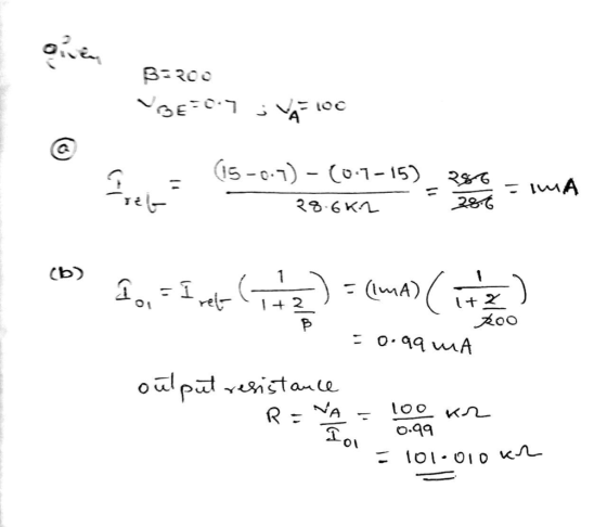
 2. In the following current mirror circuit, Vcc -10V, and the three transistors, Q1, Q2, Q3, have the same saturation current (i.e.,IssIs), and with V for active mode is 0.7V. Then, the three beta values are given by: β91-100, ßQ2-50, and ßQ3-200. The thermal voltage is ντ-25mV. Assuming that you need an output current of i1mA: ref db (a) Find the collector, base, and emitter current for all three Q1 O2 transistors when ia 1mA. (b) Find the refern ie....
An analogue amplifier circuit is shown in Figure 1 below. VDD Q5 15V JL - Vout...
 An analogue amplifier circuit is shown in Figure 1 below. VDD Q5 15V JL - Vout Irer RI Vina JET T7T Figure 1 Integrated amplifier circuit. Circuit Data: Vpp = 15 V, IREF = I1 = I2 = 1.0 mA Transistor Data: Q1: NMOS, un Cox = 80 A/V?, W/L = 100 um/0.8 um, Vtn = 0.8 V, L = 0.10 um/V Q2: NPN BJT, B = 100, Vbe = 0.7 V, VA = 150 V Q3, Q4: NMOS, un...
2. BJT Current Mirror (10) In the following circuit that is powered by Vcc=5.7 V and...
 2. BJT Current Mirror (10) In the following circuit that is powered by Vcc=5.7 V and -Vee = -5.7 V, the BJTs have infinite common-emitter DC current gains ( = 50 for each BJT). The BE junctions have a same forward biasing voltage of 0.7 V. Find I, V, V2, V3, V. for R= 5 k 2. +5.7 V Os+
(12 points) Consider the following MOS current mirror circuit. Let IREF-45 μΑ, k, = 25 ㎂/V2,...
 (12 points) Consider the following MOS current mirror circuit. Let IREF-45 μΑ, k, = 25 ㎂/V2, Vtn = 0.75 V, and λ = 0.01 V-1. The indicated ratios are the W/L for the individual transistors. Find the values of all three output currents. a) O +10 V +8 V +12 V IREF 1o 02 04 10 20 40 4 M2 4
Beta = 100 10 V IRE R3 Fig. 1: A current source and mirror circuits using...
 Beta = 100
10 V IRE R3 Fig. 1: A current source and mirror circuits using npn BJTS Design the current source and mirror circuit in Fig. 1 such that IREF = 10 mA (13%) nominally. Use supply of Vcc = 10 V, and use an average value for ß that you found in your previous experiments or that from the datasheet. Find the value of R, that satisfies the design requirements. In your pre- lab, perform the following: 1....
Beta = 100
10 V IRE R3 Fig. 1: A current source and mirror circuits using npn BJTS Design the current source and mirror circuit in Fig. 1 such that IREF = 10 mA (13%) nominally. Use supply of Vcc = 10 V, and use an average value for ß that you found in your previous experiments or that from the datasheet. Find the value of R, that satisfies the design requirements. In your pre- lab, perform the following: 1....
) The current-mirror circuit shown in Figure 3 utilizes pnp transistors having Isl 10-5A and/s2-2...
 ) The current-mirror circuit shown in Figure 3 utilizes pnp transistors having Isl 10-5A and/s2-2x10-5A for transistors Q1 and Q2 respectively and for both transistors a β 50, and |Val 10 V to source a current at Vo.It is required to design the circuit to provide an output current oflo= 1 mA at Vo = 2 V. What values of REF and R are needed? 0i 02 /REF lo
) The current-mirror circuit shown in Figure 3 utilizes pnp transistors...
) The current-mirror circuit shown in Figure 3 utilizes pnp transistors having Isl 10-5A and/s2-2x10-5A for transistors Q1 and Q2 respectively and for both transistors a β 50, and |Val 10 V to source a current at Vo.It is required to design the circuit to provide an output current oflo= 1 mA at Vo = 2 V. What values of REF and R are needed? 0i 02 /REF lo
) The current-mirror circuit shown in Figure 3 utilizes pnp transistors...
These questions refer to the BJT current mirror shown below with Iref = 100 UA (“u”...
 These questions refer to the BJT current mirror shown below with Iref = 100 UA (“u” = micro). All transistors have the same ß (beta) and VA given in questions. All output branches go to some load (dashed lines) and then to Vcc = 5 V. The area of each transistor is indicated in the figure: Qı has area “A”, Q2 has area 2A, etc. 5V Iref Io2 Io3 104 R Q2 Q3 Q4 Q1 А 2A 4A 6A Assuming...
Problem 5: 13 pts The circuit shown below is called a current mirror. Essentially the output curr...
 Note: VDD = VSS = 5V, not VDD = -VSS = 5V
Problem 5: 13 pts The circuit shown below is called a current mirror. Essentially the output current Ip2 is multiples of the input current Ip1. Both transistors have the same VT = 1V. Transistor Q2 has k2 that is five times ki (transistor Q1 constant). Let iD2 ID1 02 V. (a) Find the value of R that makes the output current Ip2 0.5mA (assume Q2 is in SAT)....
Note: VDD = VSS = 5V, not VDD = -VSS = 5V
Problem 5: 13 pts The circuit shown below is called a current mirror. Essentially the output current Ip2 is multiples of the input current Ip1. Both transistors have the same VT = 1V. Transistor Q2 has k2 that is five times ki (transistor Q1 constant). Let iD2 ID1 02 V. (a) Find the value of R that makes the output current Ip2 0.5mA (assume Q2 is in SAT)....
11.41 O The circuit of Fig. P11.41 represents the inter- nal circuitry of a simple BJT...
 11.41 O The circuit of Fig. P11.41 represents the inter- nal circuitry of a simple BJT operational amplifier. In answering the following questions, use appropriate en- gineering approximations where required. Assume the BJTs in the circuit to be matched and to have the fol- lowing parameters: Cli = 1 pF, VA 00, VBE = 0.7 V, Vsat 0.2 V,尾= 200, and η = 1 . Find the bias currents through each BJT and the bias voltages of nodes A, B,...
 Ignore PSpice Simulation
Design the BJT current mirror shown in Figure 1 to replicate a 1 mA reference current at the collector of 02. Assume a scale current of 6.7 fA, V 74 V, and B-200. 1. Determine Ri such that IREF- 1 mA is the current, Ic, flowing into the collector of Qi 2. Calculate Io/IREF, where Io- Ic2. 3. Simulate the circuit in Figure 1 in PSpice. Use the SEDRA_LIB library for the Q2N3904 and enter the appropriate...
Ignore PSpice Simulation
Design the BJT current mirror shown in Figure 1 to replicate a 1 mA reference current at the collector of 02. Assume a scale current of 6.7 fA, V 74 V, and B-200. 1. Determine Ri such that IREF- 1 mA is the current, Ic, flowing into the collector of Qi 2. Calculate Io/IREF, where Io- Ic2. 3. Simulate the circuit in Figure 1 in PSpice. Use the SEDRA_LIB library for the Q2N3904 and enter the appropriate...
 2. In the following current mirror circuit, Vcc -10V, and the three transistors, Q1, Q2, Q3, have the same saturation current (i.e.,IssIs), and with V for active mode is 0.7V. Then, the three beta values are given by: β91-100, ßQ2-50, and ßQ3-200. The thermal voltage is ντ-25mV. Assuming that you need an output current of i1mA: ref db (a) Find the collector, base, and emitter current for all three Q1 O2 transistors when ia 1mA. (b) Find the refern ie....
 An analogue amplifier circuit is shown in Figure 1 below. VDD Q5 15V JL - Vout Irer RI Vina JET T7T Figure 1 Integrated amplifier circuit. Circuit Data: Vpp = 15 V, IREF = I1 = I2 = 1.0 mA Transistor Data: Q1: NMOS, un Cox = 80 A/V?, W/L = 100 um/0.8 um, Vtn = 0.8 V, L = 0.10 um/V Q2: NPN BJT, B = 100, Vbe = 0.7 V, VA = 150 V Q3, Q4: NMOS, un...
 2. BJT Current Mirror (10) In the following circuit that is powered by Vcc=5.7 V and -Vee = -5.7 V, the BJTs have infinite common-emitter DC current gains ( = 50 for each BJT). The BE junctions have a same forward biasing voltage of 0.7 V. Find I, V, V2, V3, V. for R= 5 k 2. +5.7 V Os+
 (12 points) Consider the following MOS current mirror circuit. Let IREF-45 μΑ, k, = 25 ㎂/V2, Vtn = 0.75 V, and λ = 0.01 V-1. The indicated ratios are the W/L for the individual transistors. Find the values of all three output currents. a) O +10 V +8 V +12 V IREF 1o 02 04 10 20 40 4 M2 4
 Beta = 100
10 V IRE R3 Fig. 1: A current source and mirror circuits using npn BJTS Design the current source and mirror circuit in Fig. 1 such that IREF = 10 mA (13%) nominally. Use supply of Vcc = 10 V, and use an average value for ß that you found in your previous experiments or that from the datasheet. Find the value of R, that satisfies the design requirements. In your pre- lab, perform the following: 1....
Beta = 100
10 V IRE R3 Fig. 1: A current source and mirror circuits using npn BJTS Design the current source and mirror circuit in Fig. 1 such that IREF = 10 mA (13%) nominally. Use supply of Vcc = 10 V, and use an average value for ß that you found in your previous experiments or that from the datasheet. Find the value of R, that satisfies the design requirements. In your pre- lab, perform the following: 1....
 ) The current-mirror circuit shown in Figure 3 utilizes pnp transistors having Isl 10-5A and/s2-2x10-5A for transistors Q1 and Q2 respectively and for both transistors a β 50, and |Val 10 V to source a current at Vo.It is required to design the circuit to provide an output current oflo= 1 mA at Vo = 2 V. What values of REF and R are needed? 0i 02 /REF lo
) The current-mirror circuit shown in Figure 3 utilizes pnp transistors...
) The current-mirror circuit shown in Figure 3 utilizes pnp transistors having Isl 10-5A and/s2-2x10-5A for transistors Q1 and Q2 respectively and for both transistors a β 50, and |Val 10 V to source a current at Vo.It is required to design the circuit to provide an output current oflo= 1 mA at Vo = 2 V. What values of REF and R are needed? 0i 02 /REF lo
) The current-mirror circuit shown in Figure 3 utilizes pnp transistors...
 These questions refer to the BJT current mirror shown below with Iref = 100 UA (“u” = micro). All transistors have the same ß (beta) and VA given in questions. All output branches go to some load (dashed lines) and then to Vcc = 5 V. The area of each transistor is indicated in the figure: Qı has area “A”, Q2 has area 2A, etc. 5V Iref Io2 Io3 104 R Q2 Q3 Q4 Q1 А 2A 4A 6A Assuming...
 Note: VDD = VSS = 5V, not VDD = -VSS = 5V
Problem 5: 13 pts The circuit shown below is called a current mirror. Essentially the output current Ip2 is multiples of the input current Ip1. Both transistors have the same VT = 1V. Transistor Q2 has k2 that is five times ki (transistor Q1 constant). Let iD2 ID1 02 V. (a) Find the value of R that makes the output current Ip2 0.5mA (assume Q2 is in SAT)....
Note: VDD = VSS = 5V, not VDD = -VSS = 5V
Problem 5: 13 pts The circuit shown below is called a current mirror. Essentially the output current Ip2 is multiples of the input current Ip1. Both transistors have the same VT = 1V. Transistor Q2 has k2 that is five times ki (transistor Q1 constant). Let iD2 ID1 02 V. (a) Find the value of R that makes the output current Ip2 0.5mA (assume Q2 is in SAT)....
 11.41 O The circuit of Fig. P11.41 represents the inter- nal circuitry of a simple BJT operational amplifier. In answering the following questions, use appropriate en- gineering approximations where required. Assume the BJTs in the circuit to be matched and to have the fol- lowing parameters: Cli = 1 pF, VA 00, VBE = 0.7 V, Vsat 0.2 V,尾= 200, and η = 1 . Find the bias currents through each BJT and the bias voltages of nodes A, B,...
Most questions answered within 3 hours.
-
Where is the error in this code sequence?
String s1 = "Hello";
String s2 = "ello";...
asked 10 months ago -
Financial data for Joel de Paris, Inc., for last year
follow:
Joel de Paris, Inc.
Balance...
asked 10 months ago -
Consider this reaction:
Al2(SO4)3 (aq)+ BaCl3
(aq) Al2Cl6 (aq)- +
3BaSO4(s) . What is the...
asked 10 months ago -
Suppose that Savneet is considering increasing her
recent random sample from 20 car rentals to 40...
asked 10 months ago -
Trucks arrive at an unloading terminal at an average rate of 120
per hour.
Trucks arrive...
asked 10 months ago -
Why are methanol and ethanol completely soluble in water while
octanol is not very little soluble....
asked 10 months ago -
A facilities manager at a university reads in a research report
that the mean amount of...
asked 10 months ago -
When the CuSO4 is rehydrated by adding water to the anhydrous
compound, is this an endothermic...
asked 10 months ago -
A ray of sunlight is passing from diamond into crown glass; the
angle of incidence is...
asked 10 months ago -
A block of mass 0.249 kg is placed on top of a light, vertical
spring of...
asked 10 months ago -
how do the kidneys compensate in the presences of acidosis
a) trigger hyperventilate
b) reserve acid...
asked 10 months ago -
Question 501 pts
The rental rate of capital to the firm increases. Which of the
following...
asked 10 months ago