Write the VHDL code for RS Flip flop.
Write the VHDL code for RS Flip flop.
Homework Answers
Truth table for RS Flip Flop
Q R S Q(N+1)
0 0 0 0(Memory state same as Q)
0 0 1 1
0 1 0 0
0 1 1 UNKNOWN
1 0 0 1(Memory state same as Q)
1 0 1 0
1 1 0 1
1 1 1 UNKNOWN
CODE BELOW
library ieee;
use ieee. std_logic_1164.all;
entity SR-FF is
PORT( S,R,CLOCK: in std_logic ; Q , QBAR: out std_logic);
end SR-FF;
Architecture behavioral of SR-FF is
begin
PROCESS(CLOCK)
variable x: std_logic;
begin
if(CLOCK='1' and CLOCK'EVENT) then
if(S='0' and R='0')then
x:=x;
elsif(S='1' and R='1')then
x:='Z';
elsif(S='0' and R='1')then
x:='0';
else
x:='1';
end if;
end if;
Q<=x;
QBAR<=not x;
end PROCESS;
end behavioral
AIM: Write a VHDL code for IC7474a positive edge triggering D flip flop. TITLE: IC7474a positive...
 AIM: Write a VHDL code for IC7474a positive edge triggering D flip flop. TITLE: IC7474a positive edge triggering D flip flop. CIRCUIT DIAGRAM: pr_jb clr_1 D clk D Qn D
3. Answer the following questions about a data flip-flop (D-Flip Flop): a) (4 ps) Write the VHDL required to define a rising-edge triggered (RET) D-Flip Flop with additional clock enable (CEN) an...
 3. Answer the following questions about a data flip-flop (D-Flip Flop): a) (4 ps) Write the VHDL required to define a rising-edge triggered (RET) D-Flip Flop with additional clock enable (CEN) and reset inputs. Your reset may be synchronous or asynchronous. Assume any input, output, or signal variables that you require have already been declared in VHDL (you do not have to write the declarations for these) b) [I pal ls your reset syachronous or asynchronous for the D-Flip Flop...
Use your answer from above to modify the VHDL code provided for the D Flip-Flop in...
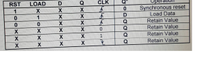 Use your answer from above to modify the VHDL code provided for
the D Flip-Flop in Section
4.3 to implement the new synchronous reset and load functions.
Simulate functionality.
RST LOAD CLK Synchronous reset Load Data Retain Value Retain Value Retain Value Retain Value
Use your answer from above to modify the VHDL code provided for
the D Flip-Flop in Section
4.3 to implement the new synchronous reset and load functions.
Simulate functionality.
RST LOAD CLK Synchronous reset Load Data Retain Value Retain Value Retain Value Retain Value
Could you please give me the T-Flip Flop and also 4-bit Binary Ripple Counter VHDL structural code with testbench
Could you please give me the T-Flip Flop and also 4-bit Binary Ripple Counter VHDL structural code with testbench
Write 3-bit Gray code using jk-flip flop in verilog (behavioral code)
write 3-bit Gray code using jk-flip flop in verilog (behavioral code)
please dont write the VHDL code on paper just copy and paste it from the program...
 please dont write the VHDL code on paper just copy and paste
it from the program
Q1 K101 Fig. 2 (b) Use the structural design style to write the VHDL code (entity and architecture) to describe the circuit in Fig. 2 if the entity of the JK flip-flop is as shown below: entity JKYT is port( Q. NO: out atd logies CLK, CLR, J, K instd_logie); and JKPF; (5 marks)
please dont write the VHDL code on paper just copy and paste
it from the program
Q1 K101 Fig. 2 (b) Use the structural design style to write the VHDL code (entity and architecture) to describe the circuit in Fig. 2 if the entity of the JK flip-flop is as shown below: entity JKYT is port( Q. NO: out atd logies CLK, CLR, J, K instd_logie); and JKPF; (5 marks)
Using verilog code, write the testbench and design for a D- Flip Flop (latch)
Using verilog code, write the testbench and design for a D- Flip Flop (latch)
.For the following circuit, do: RR3R2R, Ro G G3G2G,Go Write structural VHDL code. Create two files:...
 .For the following circuit, do: RR3R2R, Ro G G3G2G,Go Write structural VHDL code. Create two files: i) flip flop, ii) top file (where you will interconnect the flip flops and the logic gates). Provide a printout. (10 pts) Write a VHDL testbench according to the timing diagram shown below. Complete the timing diagram by simulating your circuit (Behavioral Simulation). The clock frequency must be 100 MHz with 50% duty cycle. Provide a printout. (15 pts) Ro R1 R2 Ro resetn...
Prelab Work 1. Write and simulate a Verilog code of divide by 2 using D Flip Flop во OO F4 F3 F5 ...
 can you do this fast please
Prelab Work 1. Write and simulate a Verilog code of divide by 2 using D Flip Flop во OO F4 F3 F5 F7 F8 F9 sk
Prelab Work 1. Write and simulate a Verilog code of divide by 2 using D Flip Flop во OO F4 F3 F5 F7 F8 F9 sk
can you do this fast please
Prelab Work 1. Write and simulate a Verilog code of divide by 2 using D Flip Flop во OO F4 F3 F5 F7 F8 F9 sk
Prelab Work 1. Write and simulate a Verilog code of divide by 2 using D Flip Flop во OO F4 F3 F5 F7 F8 F9 sk
21.When a clocked RS flip-flop circuit is in its set state, the output is A. Q...
21.When a clocked RS flip-flop circuit is in its set state, the output is A. Q = 0; Q = 1. B. Q = 0; Q = 0. C. Q = 1; Q = 0. D. Q = 1; Q = 1. 22. An encoding matrix is used to A. convert the comparator outputs of an A/D to a digital word. B. convert digital to analog signals. C. do binary to hexadecimal conversion. D. represent all of the values of...
 AIM: Write a VHDL code for IC7474a positive edge triggering D flip flop. TITLE: IC7474a positive edge triggering D flip flop. CIRCUIT DIAGRAM: pr_jb clr_1 D clk D Qn D
 3. Answer the following questions about a data flip-flop (D-Flip Flop): a) (4 ps) Write the VHDL required to define a rising-edge triggered (RET) D-Flip Flop with additional clock enable (CEN) and reset inputs. Your reset may be synchronous or asynchronous. Assume any input, output, or signal variables that you require have already been declared in VHDL (you do not have to write the declarations for these) b) [I pal ls your reset syachronous or asynchronous for the D-Flip Flop...
 Use your answer from above to modify the VHDL code provided for
the D Flip-Flop in Section
4.3 to implement the new synchronous reset and load functions.
Simulate functionality.
RST LOAD CLK Synchronous reset Load Data Retain Value Retain Value Retain Value Retain Value
Use your answer from above to modify the VHDL code provided for
the D Flip-Flop in Section
4.3 to implement the new synchronous reset and load functions.
Simulate functionality.
RST LOAD CLK Synchronous reset Load Data Retain Value Retain Value Retain Value Retain Value
 please dont write the VHDL code on paper just copy and paste
it from the program
Q1 K101 Fig. 2 (b) Use the structural design style to write the VHDL code (entity and architecture) to describe the circuit in Fig. 2 if the entity of the JK flip-flop is as shown below: entity JKYT is port( Q. NO: out atd logies CLK, CLR, J, K instd_logie); and JKPF; (5 marks)
please dont write the VHDL code on paper just copy and paste
it from the program
Q1 K101 Fig. 2 (b) Use the structural design style to write the VHDL code (entity and architecture) to describe the circuit in Fig. 2 if the entity of the JK flip-flop is as shown below: entity JKYT is port( Q. NO: out atd logies CLK, CLR, J, K instd_logie); and JKPF; (5 marks)
 .For the following circuit, do: RR3R2R, Ro G G3G2G,Go Write structural VHDL code. Create two files: i) flip flop, ii) top file (where you will interconnect the flip flops and the logic gates). Provide a printout. (10 pts) Write a VHDL testbench according to the timing diagram shown below. Complete the timing diagram by simulating your circuit (Behavioral Simulation). The clock frequency must be 100 MHz with 50% duty cycle. Provide a printout. (15 pts) Ro R1 R2 Ro resetn...
 can you do this fast please
Prelab Work 1. Write and simulate a Verilog code of divide by 2 using D Flip Flop во OO F4 F3 F5 F7 F8 F9 sk
Prelab Work 1. Write and simulate a Verilog code of divide by 2 using D Flip Flop во OO F4 F3 F5 F7 F8 F9 sk
can you do this fast please
Prelab Work 1. Write and simulate a Verilog code of divide by 2 using D Flip Flop во OO F4 F3 F5 F7 F8 F9 sk
Prelab Work 1. Write and simulate a Verilog code of divide by 2 using D Flip Flop во OO F4 F3 F5 F7 F8 F9 sk
Most questions answered within 3 hours.
-
Where is the error in this code sequence?
String s1 = "Hello";
String s2 = "ello";...
asked 11 months ago -
Financial data for Joel de Paris, Inc., for last year
follow:
Joel de Paris, Inc.
Balance...
asked 11 months ago -
Consider this reaction:
Al2(SO4)3 (aq)+ BaCl3
(aq) Al2Cl6 (aq)- +
3BaSO4(s) . What is the...
asked 11 months ago -
Suppose that Savneet is considering increasing her
recent random sample from 20 car rentals to 40...
asked 11 months ago -
Trucks arrive at an unloading terminal at an average rate of 120
per hour.
Trucks arrive...
asked 11 months ago -
Why are methanol and ethanol completely soluble in water while
octanol is not very little soluble....
asked 11 months ago -
A facilities manager at a university reads in a research report
that the mean amount of...
asked 11 months ago -
When the CuSO4 is rehydrated by adding water to the anhydrous
compound, is this an endothermic...
asked 11 months ago -
A ray of sunlight is passing from diamond into crown glass; the
angle of incidence is...
asked 11 months ago -
A block of mass 0.249 kg is placed on top of a light, vertical
spring of...
asked 11 months ago -
how do the kidneys compensate in the presences of acidosis
a) trigger hyperventilate
b) reserve acid...
asked 11 months ago -
Question 501 pts
The rental rate of capital to the firm increases. Which of the
following...
asked 11 months ago