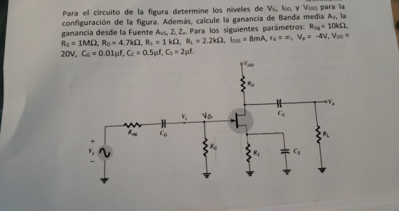
For the circuit. Find Vg, Idq and Vgsq for the configuration. Calculate the middle band gain Av and Avs, Zi and Zo.
Rsig =10kohm
Rg = 1Mohm
Rd= 4.7kohm
Rs = 1kohm
RL= 2.2kohm
Idss = 8mA
rd = infinite
Vp = -4V
Vdd = 20V
Cg = 0.01micro F
Cc = 0.5 micro F
Cs = 2 micro F
Homework Answers
Request Answer!
We need at least 10 more requests to produce the answer.
0 / 10 have requested this problem solution
The more requests, the faster the answer.
Add Answer to:
For the circuit. Find Vg, Idq and Vgsq for the
configuration. Calculate the middle band gain...
Determine the lower and upper cutoff frequency for the network. Sketch the frequency response using bode plot 2. A self-biased n-channel JFET Amplifier with C1(input)-0.01uF C2(bypass)-2uF C3(...
 Determine the lower and upper cutoff frequency for the network.
Sketch the frequency response using bode plot
2. A self-biased n-channel JFET Amplifier with C1(input)-0.01uF C2(bypass)-2uF C3(output)-0.5uF VDD 20V Rsig- 10kQ RG-1M Ω RD-4.7k Q IDSS-8mA VGS(off-AV Cgd-2pF Cgs-4pF Cds-0.5pF Cwo-6pF RL-2.2k Ω Rc rQi=120 0.47uF R, 04uF 0.82Ω R: 2. A self-biased n-channel JFET Amplifier with C1 (input)=001uF C2bypass)-2uF C3(output):0.5UF VDD-20V Rsige 10kΩ RG-1M Ω RD-4.7k Ω IDSS-BmA VGS(off)-4V Cgd-2pF Cds-0.5pF Cwi-5pF RL-2.2k Ω
2. A self-biased n-channel JFET...
Determine the lower and upper cutoff frequency for the network.
Sketch the frequency response using bode plot
2. A self-biased n-channel JFET Amplifier with C1(input)-0.01uF C2(bypass)-2uF C3(output)-0.5uF VDD 20V Rsig- 10kQ RG-1M Ω RD-4.7k Q IDSS-8mA VGS(off-AV Cgd-2pF Cgs-4pF Cds-0.5pF Cwo-6pF RL-2.2k Ω Rc rQi=120 0.47uF R, 04uF 0.82Ω R: 2. A self-biased n-channel JFET Amplifier with C1 (input)=001uF C2bypass)-2uF C3(output):0.5UF VDD-20V Rsige 10kΩ RG-1M Ω RD-4.7k Ω IDSS-BmA VGS(off)-4V Cgd-2pF Cds-0.5pF Cwi-5pF RL-2.2k Ω
2. A self-biased n-channel JFET...
Problem 3: Design Problem On Figure P3a, you have a Common Source (CS) n-channel MOSFET amplifier....
 Problem 3: Design Problem On Figure P3a, you have a Common Source (CS) n-channel MOSFET amplifier. Notice the absence of a source resistor Rsig and load resistor R. If we know how the present amplifier (the one on Figure P3a) behaves without Rsig and RL, we can infer its behaviors if Rsig and R were to be added. design the amplifier circuit on Figure P3a, i.e., you have to find appropriate values for RGj You are to RG,, RD, and...
 Determine the lower and upper cutoff frequency for the network.
Sketch the frequency response using bode plot
2. A self-biased n-channel JFET Amplifier with C1(input)-0.01uF C2(bypass)-2uF C3(output)-0.5uF VDD 20V Rsig- 10kQ RG-1M Ω RD-4.7k Q IDSS-8mA VGS(off-AV Cgd-2pF Cgs-4pF Cds-0.5pF Cwo-6pF RL-2.2k Ω Rc rQi=120 0.47uF R, 04uF 0.82Ω R: 2. A self-biased n-channel JFET Amplifier with C1 (input)=001uF C2bypass)-2uF C3(output):0.5UF VDD-20V Rsige 10kΩ RG-1M Ω RD-4.7k Ω IDSS-BmA VGS(off)-4V Cgd-2pF Cds-0.5pF Cwi-5pF RL-2.2k Ω
2. A self-biased n-channel JFET...
Determine the lower and upper cutoff frequency for the network.
Sketch the frequency response using bode plot
2. A self-biased n-channel JFET Amplifier with C1(input)-0.01uF C2(bypass)-2uF C3(output)-0.5uF VDD 20V Rsig- 10kQ RG-1M Ω RD-4.7k Q IDSS-8mA VGS(off-AV Cgd-2pF Cgs-4pF Cds-0.5pF Cwo-6pF RL-2.2k Ω Rc rQi=120 0.47uF R, 04uF 0.82Ω R: 2. A self-biased n-channel JFET Amplifier with C1 (input)=001uF C2bypass)-2uF C3(output):0.5UF VDD-20V Rsige 10kΩ RG-1M Ω RD-4.7k Ω IDSS-BmA VGS(off)-4V Cgd-2pF Cds-0.5pF Cwi-5pF RL-2.2k Ω
2. A self-biased n-channel JFET...
 Problem 3: Design Problem On Figure P3a, you have a Common Source (CS) n-channel MOSFET amplifier. Notice the absence of a source resistor Rsig and load resistor R. If we know how the present amplifier (the one on Figure P3a) behaves without Rsig and RL, we can infer its behaviors if Rsig and R were to be added. design the amplifier circuit on Figure P3a, i.e., you have to find appropriate values for RGj You are to RG,, RD, and...
Most questions answered within 3 hours.
-
Where is the error in this code sequence?
String s1 = "Hello";
String s2 = "ello";...
asked 11 months ago -
Financial data for Joel de Paris, Inc., for last year
follow:
Joel de Paris, Inc.
Balance...
asked 11 months ago -
Consider this reaction:
Al2(SO4)3 (aq)+ BaCl3
(aq) Al2Cl6 (aq)- +
3BaSO4(s) . What is the...
asked 11 months ago -
Suppose that Savneet is considering increasing her
recent random sample from 20 car rentals to 40...
asked 11 months ago -
Trucks arrive at an unloading terminal at an average rate of 120
per hour.
Trucks arrive...
asked 11 months ago -
Why are methanol and ethanol completely soluble in water while
octanol is not very little soluble....
asked 11 months ago -
A facilities manager at a university reads in a research report
that the mean amount of...
asked 11 months ago -
When the CuSO4 is rehydrated by adding water to the anhydrous
compound, is this an endothermic...
asked 11 months ago -
A ray of sunlight is passing from diamond into crown glass; the
angle of incidence is...
asked 11 months ago -
A block of mass 0.249 kg is placed on top of a light, vertical
spring of...
asked 11 months ago -
how do the kidneys compensate in the presences of acidosis
a) trigger hyperventilate
b) reserve acid...
asked 11 months ago -
Question 501 pts
The rental rate of capital to the firm increases. Which of the
following...
asked 11 months ago