Instantiate four copies of the mux2_1b in mux2_4b file. Connect the 1-bit muxes (4 mux2_1b instances)...
Instantiate four copies of the mux2_1b in mux2_4b file. Connect the 1-bit muxes (4
mux2_1b instances) with ports of mux2_4b to produce 4-bit wide 2:1 multiplexer. This is
an example of hierarchical design with reusable modules.
The mux2_4b module receives input signals a[3:0], b[3:0], sel, and generates an output
signals y[3:0].
I already have a 2_1bit mux verilog coded out but I am not getting correct results intended by what the question is asking.
//multiplexer using copies of a mux2:1
module mux2_4b(c,d,sel,y);
input [3:0]c;
input [3:0]d;
input sel;
output reg [3:0]y;
mux2
f1(.a(c[0]),.b(d[0]),.sel(sel),.x(y[0]));
mux2
f2(.a(c[1]),.b(d[1]),.sel(sel),.x(y[1]));
mux2
f3(.a(c[2]),.b(d[2]),.sel(sel),.x(y[2]));
mux2
f4(.a(c[3]),.b(d[3]),.sel(sel),.x(y[3]));
// always @(sel, c , d)
//
if (sel == 0)
// //
y <= c;
//
else
//
y <= d;
endmodule
Homework Answers
Request Answer!
We need at least 10 more requests to produce the answer.
0 / 10 have requested this problem solution
The more requests, the faster the answer.
Add Answer to:
Instantiate four copies of the mux2_1b in mux2_4b file. Connect
the 1-bit muxes (4
mux2_1b instances)...
3. From the slides and the reference materials, we see that there are two methods for...
 3. From the slides and the reference materials, we see that there are two methods for implementing logic in Verilog HDL. The circuit can be described using "Structural Verilog or "Behavioral Verilog." In Structural Verilog the structure of the circuit is defined using Boolean algebra statements. In Behavioral Verilog the circuit is defined by its behavior. Below are examples of a 2x1 multiplexer implemented using structural and behavioral Verilog. STRUCTRAL 2x1 MULTIPLEXER CODE: // Example 5a: 2-to-1 MUX using logic...
2. Let’s create a module that defines a 4:1 mux by instantiating three 2:1 muxes. Assume the modu...
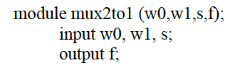 2. Let’s create a module that defines a 4:1 mux by instantiating
three 2:1 muxes. Assume the module we are going to instantiate has
the interface definition:
(a) First, write the code that would go inside the module
defined above.
(b) Now define the interface for your 4:1 mux. You can call the
module anything you want and use any variable names you want. But
think about how many inputs you’ll need.
(c) Now instantiate three instances of the 2:1...
2. Let’s create a module that defines a 4:1 mux by instantiating
three 2:1 muxes. Assume the module we are going to instantiate has
the interface definition:
(a) First, write the code that would go inside the module
defined above.
(b) Now define the interface for your 4:1 mux. You can call the
module anything you want and use any variable names you want. But
think about how many inputs you’ll need.
(c) Now instantiate three instances of the 2:1...
A specific type of bit-level manipulation consists in setting or clearing one single bit in a...
A specific type of bit-level manipulation consists in setting or clearing one single bit in a multi-bit value, given its index and its new value. This operation can be implemented in hardware by a BitSet circuit with the following interface: Input x is a 4-bit value representing the original value. Output y is a 4-bit value representing the modified value, after the bit-set operation. Input index is a 2-bit value, ranging from 0 to 3, indicating the index of the...
Please code the following in Verilog: Write the HDL gate-level hierarchical description of a four-bit adder-subtractor...
 Please code the following in Verilog:
Write the HDL gate-level hierarchical description of a four-bit adder-subtractor for unsigned binary numbers similar to the following circuit. You can instantiate the four-bit full adder described in the following example code Figure 4.13a, 4-Bit adder-subtractor without overflow Inputs: 4-Bit A, 4-Bit B, and Mode M (0-add/1-subtract) Interfaces: Carry Bits C1, C2, C3 Outputs: Carry C (1 Bit, C4), Sum S (4 bit) Bo A FA FA FA FA module Add half (input a,...
Please code the following in Verilog:
Write the HDL gate-level hierarchical description of a four-bit adder-subtractor for unsigned binary numbers similar to the following circuit. You can instantiate the four-bit full adder described in the following example code Figure 4.13a, 4-Bit adder-subtractor without overflow Inputs: 4-Bit A, 4-Bit B, and Mode M (0-add/1-subtract) Interfaces: Carry Bits C1, C2, C3 Outputs: Carry C (1 Bit, C4), Sum S (4 bit) Bo A FA FA FA FA module Add half (input a,...
2. Let's create a module that defines a 4:1 mux by instantiating three 2:1 muxes. Assume the modu...
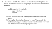 2. Let's create a module that defines a 4:1 mux by instantiating three 2:1 muxes. Assume the module we are going to instantiate has the interface definition: module mux2tol (wO,wl,s,f); input w0, wl, s; output f (a) First, write the code that would go inside the module defined above. (b) Now define the interface for your 4:1 mux. You can call the le anything you wa But think about how many inputs you'll need.
2. Let's create a module that...
2. Let's create a module that defines a 4:1 mux by instantiating three 2:1 muxes. Assume the module we are going to instantiate has the interface definition: module mux2tol (wO,wl,s,f); input w0, wl, s; output f (a) First, write the code that would go inside the module defined above. (b) Now define the interface for your 4:1 mux. You can call the le anything you wa But think about how many inputs you'll need.
2. Let's create a module that...
why its 4-to-1 mux behavioral? What does the logic circuit represented by the following Verilog module...
 why its 4-to-1 mux behavioral?
What does the logic circuit represented by the following Verilog module do, and what Verilog description style does it use? // My Verilog module #1 module mymodl ( x, d, q) input[1:0] x;input[3:0] d;output q; reg q; wire [1:0] x; wire [3:0] d; always ( x or d) begin case ( x ) 1 : q=d[1]; 2 : g=d[2]; 3 q d[3]; endcase end endmodule
why its 4-to-1 mux behavioral?
What does the logic circuit represented by the following Verilog module do, and what Verilog description style does it use? // My Verilog module #1 module mymodl ( x, d, q) input[1:0] x;input[3:0] d;output q; reg q; wire [1:0] x; wire [3:0] d; always ( x or d) begin case ( x ) 1 : q=d[1]; 2 : g=d[2]; 3 q d[3]; endcase end endmodule
Consider the circuit in Figure 1. It is a 4-bit (QQ2Q3) synchronous counter which uses four T-typ...
 Consider the circuit in Figure 1. It is a 4-bit (QQ2Q3) synchronous counter which uses four T-type flip-flops. The counter increases its value on each positive edge of the clock if the Enable signal is asserted. The counter is reset to 0 by setting the Clear signal low. You are to implement an 8-bit counter of this type Enable T Q Clock Clear Figure 1. 4-bit synchronous counter (but you need to implement 8-bit counter in this lab) Specific notes:...
2d) (10 pts) Design a 2-bit ALU using a 2-bit adder and multiplexors (muxes) for the...
 2d) (10 pts) Design a 2-bit ALU using a 2-bit adder and multiplexors (muxes) for the following operation table W X ALU operation 0 0 A +2 0 1 A & B (bit-wise) 1 0 B >> 1 (filled with 0) A-B Note: To make a connection, instead of drawing a line to make a connection, write a signal at each mux input using al, a, b1, b0, 0, or 1 and/or logic gates if needed. а0 b1 bo si...
Objective: Creating a register file (memory) using Verilog. The register file is made up of four registers and each...
 Objective: Creating a register file (memory) using Verilog. The register file is made up of four registers and each register holds one nibble (half a byte, i.e., four bits) 3. Create a D flip-flop AD flip-flop holds 1 bit of data, and it only changes its data when the clock changes. We want a positive edge triggered flip-flop. Design your Verilog D flip-flop, so we will create them now. Enter the 2 to 4 line decoder. We will need two...
Building and testing basic combinational circuits using Verilog HDL Description: Build and test the following circuits using gate-level modeling in Verilog HDL 1.3-input majority function 2.Condition...
 Building and testing basic combinational circuits using Verilog HDL Description: Build and test the following circuits using gate-level modeling in Verilog HDL 1.3-input majority function 2.Conditional inverter (see the table below: x - control input, y -data input). Do NOT use XOR gates for the implementation. Output 3. Two-input multiplexer (see the table below: x.y -data inputs, z- control input) Output 4. 1-bit half adder. 5. 1-bit full adder by cascading two half adders 6.1-bit full adder directly (as in...
 3. From the slides and the reference materials, we see that there are two methods for implementing logic in Verilog HDL. The circuit can be described using "Structural Verilog or "Behavioral Verilog." In Structural Verilog the structure of the circuit is defined using Boolean algebra statements. In Behavioral Verilog the circuit is defined by its behavior. Below are examples of a 2x1 multiplexer implemented using structural and behavioral Verilog. STRUCTRAL 2x1 MULTIPLEXER CODE: // Example 5a: 2-to-1 MUX using logic...
 2. Let’s create a module that defines a 4:1 mux by instantiating
three 2:1 muxes. Assume the module we are going to instantiate has
the interface definition:
(a) First, write the code that would go inside the module
defined above.
(b) Now define the interface for your 4:1 mux. You can call the
module anything you want and use any variable names you want. But
think about how many inputs you’ll need.
(c) Now instantiate three instances of the 2:1...
2. Let’s create a module that defines a 4:1 mux by instantiating
three 2:1 muxes. Assume the module we are going to instantiate has
the interface definition:
(a) First, write the code that would go inside the module
defined above.
(b) Now define the interface for your 4:1 mux. You can call the
module anything you want and use any variable names you want. But
think about how many inputs you’ll need.
(c) Now instantiate three instances of the 2:1...
 Please code the following in Verilog:
Write the HDL gate-level hierarchical description of a four-bit adder-subtractor for unsigned binary numbers similar to the following circuit. You can instantiate the four-bit full adder described in the following example code Figure 4.13a, 4-Bit adder-subtractor without overflow Inputs: 4-Bit A, 4-Bit B, and Mode M (0-add/1-subtract) Interfaces: Carry Bits C1, C2, C3 Outputs: Carry C (1 Bit, C4), Sum S (4 bit) Bo A FA FA FA FA module Add half (input a,...
Please code the following in Verilog:
Write the HDL gate-level hierarchical description of a four-bit adder-subtractor for unsigned binary numbers similar to the following circuit. You can instantiate the four-bit full adder described in the following example code Figure 4.13a, 4-Bit adder-subtractor without overflow Inputs: 4-Bit A, 4-Bit B, and Mode M (0-add/1-subtract) Interfaces: Carry Bits C1, C2, C3 Outputs: Carry C (1 Bit, C4), Sum S (4 bit) Bo A FA FA FA FA module Add half (input a,...
 2. Let's create a module that defines a 4:1 mux by instantiating three 2:1 muxes. Assume the module we are going to instantiate has the interface definition: module mux2tol (wO,wl,s,f); input w0, wl, s; output f (a) First, write the code that would go inside the module defined above. (b) Now define the interface for your 4:1 mux. You can call the le anything you wa But think about how many inputs you'll need.
2. Let's create a module that...
2. Let's create a module that defines a 4:1 mux by instantiating three 2:1 muxes. Assume the module we are going to instantiate has the interface definition: module mux2tol (wO,wl,s,f); input w0, wl, s; output f (a) First, write the code that would go inside the module defined above. (b) Now define the interface for your 4:1 mux. You can call the le anything you wa But think about how many inputs you'll need.
2. Let's create a module that...
 why its 4-to-1 mux behavioral?
What does the logic circuit represented by the following Verilog module do, and what Verilog description style does it use? // My Verilog module #1 module mymodl ( x, d, q) input[1:0] x;input[3:0] d;output q; reg q; wire [1:0] x; wire [3:0] d; always ( x or d) begin case ( x ) 1 : q=d[1]; 2 : g=d[2]; 3 q d[3]; endcase end endmodule
why its 4-to-1 mux behavioral?
What does the logic circuit represented by the following Verilog module do, and what Verilog description style does it use? // My Verilog module #1 module mymodl ( x, d, q) input[1:0] x;input[3:0] d;output q; reg q; wire [1:0] x; wire [3:0] d; always ( x or d) begin case ( x ) 1 : q=d[1]; 2 : g=d[2]; 3 q d[3]; endcase end endmodule
 Consider the circuit in Figure 1. It is a 4-bit (QQ2Q3) synchronous counter which uses four T-type flip-flops. The counter increases its value on each positive edge of the clock if the Enable signal is asserted. The counter is reset to 0 by setting the Clear signal low. You are to implement an 8-bit counter of this type Enable T Q Clock Clear Figure 1. 4-bit synchronous counter (but you need to implement 8-bit counter in this lab) Specific notes:...
 2d) (10 pts) Design a 2-bit ALU using a 2-bit adder and multiplexors (muxes) for the following operation table W X ALU operation 0 0 A +2 0 1 A & B (bit-wise) 1 0 B >> 1 (filled with 0) A-B Note: To make a connection, instead of drawing a line to make a connection, write a signal at each mux input using al, a, b1, b0, 0, or 1 and/or logic gates if needed. а0 b1 bo si...
 Objective: Creating a register file (memory) using Verilog. The register file is made up of four registers and each register holds one nibble (half a byte, i.e., four bits) 3. Create a D flip-flop AD flip-flop holds 1 bit of data, and it only changes its data when the clock changes. We want a positive edge triggered flip-flop. Design your Verilog D flip-flop, so we will create them now. Enter the 2 to 4 line decoder. We will need two...
 Building and testing basic combinational circuits using Verilog HDL Description: Build and test the following circuits using gate-level modeling in Verilog HDL 1.3-input majority function 2.Conditional inverter (see the table below: x - control input, y -data input). Do NOT use XOR gates for the implementation. Output 3. Two-input multiplexer (see the table below: x.y -data inputs, z- control input) Output 4. 1-bit half adder. 5. 1-bit full adder by cascading two half adders 6.1-bit full adder directly (as in...
Most questions answered within 3 hours.
-
Where is the error in this code sequence?
String s1 = "Hello";
String s2 = "ello";...
asked 11 months ago -
Financial data for Joel de Paris, Inc., for last year
follow:
Joel de Paris, Inc.
Balance...
asked 11 months ago -
Consider this reaction:
Al2(SO4)3 (aq)+ BaCl3
(aq) Al2Cl6 (aq)- +
3BaSO4(s) . What is the...
asked 11 months ago -
Suppose that Savneet is considering increasing her
recent random sample from 20 car rentals to 40...
asked 11 months ago -
Trucks arrive at an unloading terminal at an average rate of 120
per hour.
Trucks arrive...
asked 11 months ago -
Why are methanol and ethanol completely soluble in water while
octanol is not very little soluble....
asked 11 months ago -
A facilities manager at a university reads in a research report
that the mean amount of...
asked 11 months ago -
When the CuSO4 is rehydrated by adding water to the anhydrous
compound, is this an endothermic...
asked 11 months ago -
A ray of sunlight is passing from diamond into crown glass; the
angle of incidence is...
asked 11 months ago -
A block of mass 0.249 kg is placed on top of a light, vertical
spring of...
asked 11 months ago -
how do the kidneys compensate in the presences of acidosis
a) trigger hyperventilate
b) reserve acid...
asked 11 months ago -
Question 501 pts
The rental rate of capital to the firm increases. Which of the
following...
asked 11 months ago