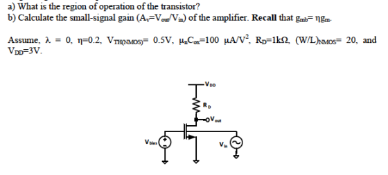
It is possible to use the bulk terminal of a transistor as an input of an amplifier. Consider the single-stage NMOS amplifier shown below.

Homework Answers
Request Answer!
We need at least 10 more requests to produce the answer.
0 / 10 have requested this problem solution
The more requests, the faster the answer.
Add Answer to:
It is possible to use the bulk terminal of a transistor as an
input of an...
In the amplifier circuit below, the transistor has the following properties:Vt =1.5V,k’n=100 microA/V2,W=2 micro m ,L=0.2...
 In the amplifier circuit below, the transistor has the following
properties:Vt =1.5V,k’n=100 microA/V2,W=2 micro m ,L=0.2 micro m,
lambda = 0V^-1
a. Find the dc values VG, VD, and VS.
b. Verify (prove) that the circuit is in the proper region of
operation for an amplifier
c. Find the transconductance value, gm
d. Draw the equivalent small-signal circuit model, replacing the
NMOS with its pi-model
e. Draw the equivalent small-signal circuit model, replacing the
NMOS with its T-model
f. Calculate...
In the amplifier circuit below, the transistor has the following
properties:Vt =1.5V,k’n=100 microA/V2,W=2 micro m ,L=0.2 micro m,
lambda = 0V^-1
a. Find the dc values VG, VD, and VS.
b. Verify (prove) that the circuit is in the proper region of
operation for an amplifier
c. Find the transconductance value, gm
d. Draw the equivalent small-signal circuit model, replacing the
NMOS with its pi-model
e. Draw the equivalent small-signal circuit model, replacing the
NMOS with its T-model
f. Calculate...
Capacitor values can be assumed to be large enough in the small-signal analysis frequency band. (Hint:...
 Capacitor values can be assumed to be large enough in the
small-signal analysis frequency band. (Hint: Consider separating
the bias and small-signal signals.) 1. Find the bias current
flowing into the transistor (λ=0) 2. Find the small-signal voltage
gain Vout/Vin value. (λ=0.1V^(-1))
Vpp=20V T VBias=3V Rp=10k Rg=90k 2 Vout VIN - HE Rsig=10812 B=1mA/V2 Vth=1V Rs=50012
Capacitor values can be assumed to be large enough in the
small-signal analysis frequency band. (Hint: Consider separating
the bias and small-signal signals.) 1. Find the bias current
flowing into the transistor (λ=0) 2. Find the small-signal voltage
gain Vout/Vin value. (λ=0.1V^(-1))
Vpp=20V T VBias=3V Rp=10k Rg=90k 2 Vout VIN - HE Rsig=10812 B=1mA/V2 Vth=1V Rs=50012
A MOSFET is wired as a common-source amplifier as shown below. The input voltage vIN is...
 A MOSFET is wired as a common-source amplifier as shown below.
The input voltage vIN is the total of the source for
biasing the circuit at its operating point (vBIAS), and
a small signal ac source providing the signal that we want to
amplify (vin). The total output voltage is
vO.
a) Assume VDD = 5?, VIN = 2?, and ? = 4?Ω
in the circuit and the MOSFET parameters are K =
0.5??/?2, VTH 1?, and ? = 0.05V-1....
A MOSFET is wired as a common-source amplifier as shown below.
The input voltage vIN is the total of the source for
biasing the circuit at its operating point (vBIAS), and
a small signal ac source providing the signal that we want to
amplify (vin). The total output voltage is
vO.
a) Assume VDD = 5?, VIN = 2?, and ? = 4?Ω
in the circuit and the MOSFET parameters are K =
0.5??/?2, VTH 1?, and ? = 0.05V-1....
QUESTION (1) Transistor Mi in this common base amplifier circuit has the following characteristics: +Vc VTH...
 QUESTION (1) Transistor Mi in this common base amplifier circuit has the following characteristics: +Vc VTH =1 V Rp R, C. K 1 mA/V2 2 0.1 R Given: Vcc 2 mA, 10 V, lbias Ct C2 0, 5 k2, RD 2 k2 RI 10 k, R2 R (12 points) a) Determine the small signal gain, vo/Vin. (4 points) b) Determine the input resistance, Rin. (4 points) c) Determine the output resistance, Ro. Useful formulae: for n-channel MOSFET triode region =...
Exercise 12.13 Derive expressions for the voltage gain, input resistance, and output resistance of the common-gate...
 Exercise 12.13 Derive expressions for the voltage gain, input resistance, and output resistance of the common-gate amplifier shown in Figure 12.29, assuming that ra is an open circuit Answer The small-signal equivalent circuit is shown in Figure 12.30. A Rin 1/(gm 1/Rs); Ro = Rp. gmR/; +VDD С2 + RL Vo CL R + Vin v(t) -Vss W Ri Rp R 8mVgs Vo Rs Vin + v(t)
Exercise 12.13 Derive expressions for the voltage gain, input resistance, and output resistance...
Exercise 12.13 Derive expressions for the voltage gain, input resistance, and output resistance of the common-gate amplifier shown in Figure 12.29, assuming that ra is an open circuit Answer The small-signal equivalent circuit is shown in Figure 12.30. A Rin 1/(gm 1/Rs); Ro = Rp. gmR/; +VDD С2 + RL Vo CL R + Vin v(t) -Vss W Ri Rp R 8mVgs Vo Rs Vin + v(t)
Exercise 12.13 Derive expressions for the voltage gain, input resistance, and output resistance...
URGENT The NMOS in the shown figure has Vt = 0.8V, kn = 5 mA/V2, and...
 URGENT
The NMOS in the shown figure has Vt = 0.8V, kn = 5 mA/V2, and VA = 40 V. The circuit also has Vdd = 5V, VSS = -5V, RG = RLD = 1 M2, and RLS = 0 A. [3 marks] Neglecting the channel length modulation effect, find the value of Rs so that the NMOS operates in saturation with Ip = 0.4 mA B. [2 marks] Neglecting the channel length modulation effect, find the largest possible value...
URGENT
The NMOS in the shown figure has Vt = 0.8V, kn = 5 mA/V2, and VA = 40 V. The circuit also has Vdd = 5V, VSS = -5V, RG = RLD = 1 M2, and RLS = 0 A. [3 marks] Neglecting the channel length modulation effect, find the value of Rs so that the NMOS operates in saturation with Ip = 0.4 mA B. [2 marks] Neglecting the channel length modulation effect, find the largest possible value...
In the CE amplifier shown below, a. Find the transistor DC operating points. Check what region...
 In the CE amplifier shown below, a. Find the transistor DC operating points. Check what region of operation the transistor is biased at. b. Calculate the small signal voltage gain, the input resistance looking into the base of the transistor, and the output resistance looking down at the collector. c. Find the small signal current gain, 으 VBE,ON = 0.6V, and β = 100, VA = 00, Base current may be ignored if possible
1 bias V. out 2 2:1 mirror 6:52 PMw Variahle 2:1 mirror S Transistor PMOS Transistor Variable NMO 1 00 0.5 0.10 35 0.5 0.20 VT (V) A (1M) L (um) Vdd is 3V The bias current is 40μΑ the bias voltag...
 1 bias V. out 2 2:1 mirror 6:52 PMw Variahle 2:1 mirror S Transistor PMOS Transistor Variable NMO 1 00 0.5 0.10 35 0.5 0.20 VT (V) A (1M) L (um) Vdd is 3V The bias current is 40μΑ the bias voltage at the rot. Vin-is2.8V, and thie voltage ut port a is O.7V. The load capacitance (CL) is Sp The NMOS current mirror is 2:1 NOTE: All 3 devices are NMOS above Include proper units for full credit and...
1. Consider NMOS transistor in the circuit that has u.Cox = 0.4 mA/V?, W/L = 25,...
 1. Consider NMOS transistor in the circuit that has u.Cox = 0.4 mA/V?, W/L = 25, and V.=0.4V. (20 pts) (a) Find the value of Vas that results in saturation mode operation with a lp current of 0.1 mA. Neglect the Early effect. (2.5 pts) +1.5 V in BRD (b) Find the value of Rp that results in a de drain voltage of 0.5V. (2.5 pts) = = = (e) Find gw and r, at the de operating point specified...
3. In Figure 3 on page 5, the DC operating point for the PNP transistor Qi...
 3. In Figure 3 on page 5, the DC operating point for the PNP transistor Qi is Ic = 0.33 mA and Vec = 2.4 V, and the DC operating point for the NMOS transistor Mi is ID = 2.81 mA and Vos = 2.92 V. Qı has B = 100, VA = 85 V at room temperature and Mi has Kn= 1 mA/V2, Vin= 1 V and 2 = 0.02 V-1. Assume that the capacitors have infinite values, and...
 In the amplifier circuit below, the transistor has the following
properties:Vt =1.5V,k’n=100 microA/V2,W=2 micro m ,L=0.2 micro m,
lambda = 0V^-1
a. Find the dc values VG, VD, and VS.
b. Verify (prove) that the circuit is in the proper region of
operation for an amplifier
c. Find the transconductance value, gm
d. Draw the equivalent small-signal circuit model, replacing the
NMOS with its pi-model
e. Draw the equivalent small-signal circuit model, replacing the
NMOS with its T-model
f. Calculate...
In the amplifier circuit below, the transistor has the following
properties:Vt =1.5V,k’n=100 microA/V2,W=2 micro m ,L=0.2 micro m,
lambda = 0V^-1
a. Find the dc values VG, VD, and VS.
b. Verify (prove) that the circuit is in the proper region of
operation for an amplifier
c. Find the transconductance value, gm
d. Draw the equivalent small-signal circuit model, replacing the
NMOS with its pi-model
e. Draw the equivalent small-signal circuit model, replacing the
NMOS with its T-model
f. Calculate...
 Capacitor values can be assumed to be large enough in the
small-signal analysis frequency band. (Hint: Consider separating
the bias and small-signal signals.) 1. Find the bias current
flowing into the transistor (λ=0) 2. Find the small-signal voltage
gain Vout/Vin value. (λ=0.1V^(-1))
Vpp=20V T VBias=3V Rp=10k Rg=90k 2 Vout VIN - HE Rsig=10812 B=1mA/V2 Vth=1V Rs=50012
Capacitor values can be assumed to be large enough in the
small-signal analysis frequency band. (Hint: Consider separating
the bias and small-signal signals.) 1. Find the bias current
flowing into the transistor (λ=0) 2. Find the small-signal voltage
gain Vout/Vin value. (λ=0.1V^(-1))
Vpp=20V T VBias=3V Rp=10k Rg=90k 2 Vout VIN - HE Rsig=10812 B=1mA/V2 Vth=1V Rs=50012
 A MOSFET is wired as a common-source amplifier as shown below.
The input voltage vIN is the total of the source for
biasing the circuit at its operating point (vBIAS), and
a small signal ac source providing the signal that we want to
amplify (vin). The total output voltage is
vO.
a) Assume VDD = 5?, VIN = 2?, and ? = 4?Ω
in the circuit and the MOSFET parameters are K =
0.5??/?2, VTH 1?, and ? = 0.05V-1....
A MOSFET is wired as a common-source amplifier as shown below.
The input voltage vIN is the total of the source for
biasing the circuit at its operating point (vBIAS), and
a small signal ac source providing the signal that we want to
amplify (vin). The total output voltage is
vO.
a) Assume VDD = 5?, VIN = 2?, and ? = 4?Ω
in the circuit and the MOSFET parameters are K =
0.5??/?2, VTH 1?, and ? = 0.05V-1....
 QUESTION (1) Transistor Mi in this common base amplifier circuit has the following characteristics: +Vc VTH =1 V Rp R, C. K 1 mA/V2 2 0.1 R Given: Vcc 2 mA, 10 V, lbias Ct C2 0, 5 k2, RD 2 k2 RI 10 k, R2 R (12 points) a) Determine the small signal gain, vo/Vin. (4 points) b) Determine the input resistance, Rin. (4 points) c) Determine the output resistance, Ro. Useful formulae: for n-channel MOSFET triode region =...
 Exercise 12.13 Derive expressions for the voltage gain, input resistance, and output resistance of the common-gate amplifier shown in Figure 12.29, assuming that ra is an open circuit Answer The small-signal equivalent circuit is shown in Figure 12.30. A Rin 1/(gm 1/Rs); Ro = Rp. gmR/; +VDD С2 + RL Vo CL R + Vin v(t) -Vss W Ri Rp R 8mVgs Vo Rs Vin + v(t)
Exercise 12.13 Derive expressions for the voltage gain, input resistance, and output resistance...
Exercise 12.13 Derive expressions for the voltage gain, input resistance, and output resistance of the common-gate amplifier shown in Figure 12.29, assuming that ra is an open circuit Answer The small-signal equivalent circuit is shown in Figure 12.30. A Rin 1/(gm 1/Rs); Ro = Rp. gmR/; +VDD С2 + RL Vo CL R + Vin v(t) -Vss W Ri Rp R 8mVgs Vo Rs Vin + v(t)
Exercise 12.13 Derive expressions for the voltage gain, input resistance, and output resistance...
 URGENT
The NMOS in the shown figure has Vt = 0.8V, kn = 5 mA/V2, and VA = 40 V. The circuit also has Vdd = 5V, VSS = -5V, RG = RLD = 1 M2, and RLS = 0 A. [3 marks] Neglecting the channel length modulation effect, find the value of Rs so that the NMOS operates in saturation with Ip = 0.4 mA B. [2 marks] Neglecting the channel length modulation effect, find the largest possible value...
URGENT
The NMOS in the shown figure has Vt = 0.8V, kn = 5 mA/V2, and VA = 40 V. The circuit also has Vdd = 5V, VSS = -5V, RG = RLD = 1 M2, and RLS = 0 A. [3 marks] Neglecting the channel length modulation effect, find the value of Rs so that the NMOS operates in saturation with Ip = 0.4 mA B. [2 marks] Neglecting the channel length modulation effect, find the largest possible value...
 In the CE amplifier shown below, a. Find the transistor DC operating points. Check what region of operation the transistor is biased at. b. Calculate the small signal voltage gain, the input resistance looking into the base of the transistor, and the output resistance looking down at the collector. c. Find the small signal current gain, 으 VBE,ON = 0.6V, and β = 100, VA = 00, Base current may be ignored if possible
 1 bias V. out 2 2:1 mirror 6:52 PMw Variahle 2:1 mirror S Transistor PMOS Transistor Variable NMO 1 00 0.5 0.10 35 0.5 0.20 VT (V) A (1M) L (um) Vdd is 3V The bias current is 40μΑ the bias voltage at the rot. Vin-is2.8V, and thie voltage ut port a is O.7V. The load capacitance (CL) is Sp The NMOS current mirror is 2:1 NOTE: All 3 devices are NMOS above Include proper units for full credit and...
 1. Consider NMOS transistor in the circuit that has u.Cox = 0.4 mA/V?, W/L = 25, and V.=0.4V. (20 pts) (a) Find the value of Vas that results in saturation mode operation with a lp current of 0.1 mA. Neglect the Early effect. (2.5 pts) +1.5 V in BRD (b) Find the value of Rp that results in a de drain voltage of 0.5V. (2.5 pts) = = = (e) Find gw and r, at the de operating point specified...
 3. In Figure 3 on page 5, the DC operating point for the PNP transistor Qi is Ic = 0.33 mA and Vec = 2.4 V, and the DC operating point for the NMOS transistor Mi is ID = 2.81 mA and Vos = 2.92 V. Qı has B = 100, VA = 85 V at room temperature and Mi has Kn= 1 mA/V2, Vin= 1 V and 2 = 0.02 V-1. Assume that the capacitors have infinite values, and...
Most questions answered within 3 hours.
-
Where is the error in this code sequence?
String s1 = "Hello";
String s2 = "ello";...
asked 11 months ago -
Financial data for Joel de Paris, Inc., for last year
follow:
Joel de Paris, Inc.
Balance...
asked 11 months ago -
Consider this reaction:
Al2(SO4)3 (aq)+ BaCl3
(aq) Al2Cl6 (aq)- +
3BaSO4(s) . What is the...
asked 11 months ago -
Suppose that Savneet is considering increasing her
recent random sample from 20 car rentals to 40...
asked 11 months ago -
Trucks arrive at an unloading terminal at an average rate of 120
per hour.
Trucks arrive...
asked 11 months ago -
Why are methanol and ethanol completely soluble in water while
octanol is not very little soluble....
asked 11 months ago -
A facilities manager at a university reads in a research report
that the mean amount of...
asked 11 months ago -
When the CuSO4 is rehydrated by adding water to the anhydrous
compound, is this an endothermic...
asked 11 months ago -
A ray of sunlight is passing from diamond into crown glass; the
angle of incidence is...
asked 11 months ago -
A block of mass 0.249 kg is placed on top of a light, vertical
spring of...
asked 11 months ago -
how do the kidneys compensate in the presences of acidosis
a) trigger hyperventilate
b) reserve acid...
asked 11 months ago -
Question 501 pts
The rental rate of capital to the firm increases. Which of the
following...
asked 11 months ago