
Homework Answers


Add Answer to:
3. In Figure 3 on page 5, the DC operating point for the PNP transistor Qi...
3. In Figure 3, the DC operating point for BJT Q, is Ici = 170 uA...
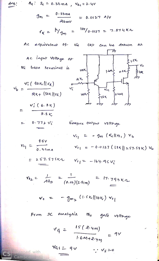
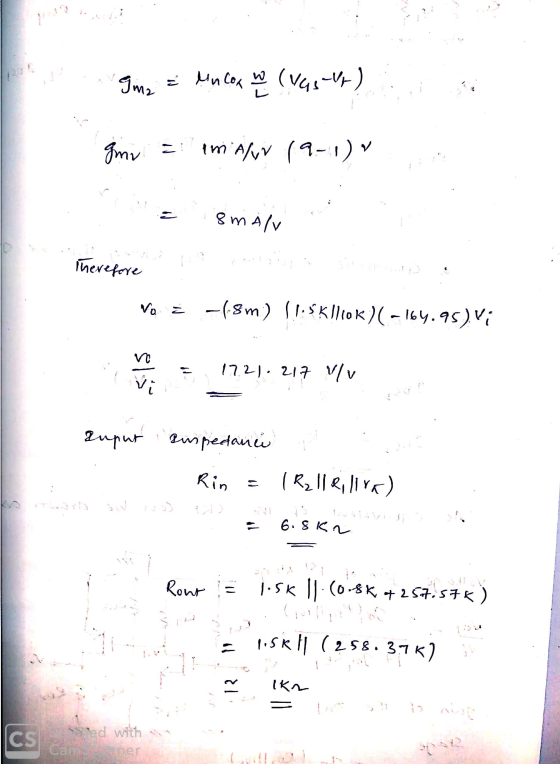
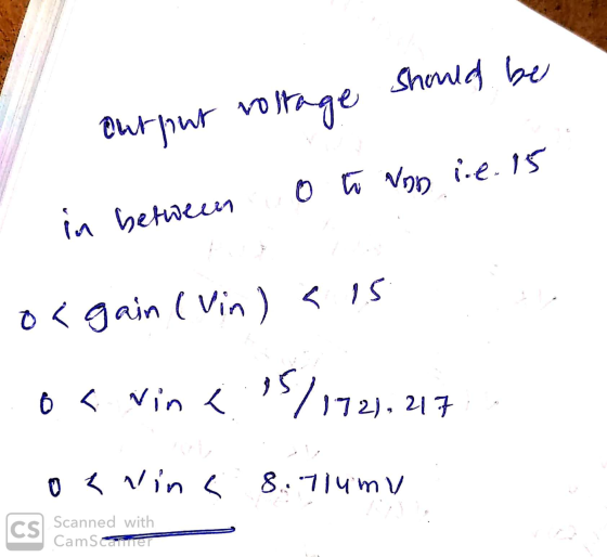
 3. In Figure 3, the DC operating point for BJT Q, is Ici = 170 uA and VCE = 4 V, and the DC operating point for BJT 02 is Ic2 = 240 A and VCE2 = 3 V. Both Q1 and Q2 have B = 100, VA-75 V at the room temperature. Assume that all the capacitors have infinite values, and all the resistors have the values as indicated in Figure 3. (a) (b) Determine the voltage gain 4....
4. For the amplifier in the figure below use the parameters in the table: +Vcc Re VBE- 0.7V, Ri- ...
 4. For the amplifier in the figure below use the parameters in the table: +Vcc Re VBE- 0.7V, Ri- 1002, R1-160k2, R2-320k2 R3-200k2, R6-40 k2, Rc-60k2, Vcc- 12V, Ry Do a) Draw the DC equivalent circuit and calculate the Q-point. c) Draw the AC equivalent circuit with the small signal model for the transistor. d) Calculate the voltage gain, Av-Vo/vi. Assume ro infinite. e) Draw the circuit to find the amplifier input resistance (Rin). Calculate Rin f Draw the circuit...
Problem 2 Consider the feedback amplifier circuit on Figure P2. The DC current gain of transistor Q3 is -100 1. What type of feedback (or what feedback topology) do we have on the circuit in Figure P...
 Problem 2 Consider the feedback amplifier circuit on Figure P2. The DC current gain of transistor Q3 is -100 1. What type of feedback (or what feedback topology) do we have on the circuit in Figure P2? 2. Draw the A-circuit. Express and compute the open-loop voltage gain A at mid-band frequency 3, Draw the γ-circuit. Express and compute the feedback factor γ 4. Express and compute the overall gain of the feedback amplifier Ap Express and compute the input...
Solve multiple choice pleassee??? with fig1 02: Choose the correct answer for the above amplifier pointleach)...
 Solve multiple choice pleassee???
with fig1
02: Choose the correct answer for the above amplifier pointleach) 1. The amplifier in figure (1) is operating in: i) Saturation mode ii) Triode mode iii) Cutoff mode 2. The configuration of the above amplifier is: i)Common Drain ii) Common Source with R, i) Common Gate 3. To measure Rin Experimentally, the added resistor (RD) should be connected to the circuit: i) in parallel with input ii)in parallel with output ii) in series with...
Solve multiple choice pleassee???
with fig1
02: Choose the correct answer for the above amplifier pointleach) 1. The amplifier in figure (1) is operating in: i) Saturation mode ii) Triode mode iii) Cutoff mode 2. The configuration of the above amplifier is: i)Common Drain ii) Common Source with R, i) Common Gate 3. To measure Rin Experimentally, the added resistor (RD) should be connected to the circuit: i) in parallel with input ii)in parallel with output ii) in series with...
5) Consider the Cascode amplifier shown below. For the NMOS transistors, kn 0.2 mA/V2, Vr,-0.5 V,...
 5) Consider the Cascode amplifier shown below. For the NMOS transistors, kn 0.2 mA/V2, Vr,-0.5 V, (W/L)-(W/L)2-5. VDD-GV and IBIAs= 1.0 mA. a) Assuming λ-0 for all transistors, find the required DC gate- source voltages of M1 and M2 (VGsı and VGs2, respectively) BIAS VD out b) Again assuming 0 M2 for all transistors, what is the minimum DC value of VouT for which the amplifier works in high-gain regime? (W/L)2 in M1 For parts c)-f), Assume -0.01 for all...
5). In this problem, you are asked to consider the ac hybrid-x model for an NMOS transistor and t...
 5). In this problem, you are asked to consider the ac hybrid-x model for an NMOS transistor and to relate the capacitors to the physical device structure. Recall the oxide capacitance per unit area ox) appears in the DC Ip-Vs relationship for triode and saturation regions. The NMOS transistor has kn-0.2 mA/V2, W 10 μm, L-I μm and μ,-1000 cm2/Vsec. a) Find the total gate-to-channel capacitance for small VDs, CG-cho. Hint: this is the parallel-plate capacitance between the gate and...
EEET255 Electronics Page 4 of6 QUESTION 3: [25 marks] Figure 3 shows a feedback amplifier circuit...
 EEET255 Electronics Page 4 of6 QUESTION 3: [25 marks] Figure 3 shows a feedback amplifier circuit R, is the source resistor, R is the feedback resistor and R, is the load resistor. The op-amp has an internal input resistance of R, an intemal output resistance R, and an internal gain of A Apply the "Systematic Analysis" method in this question. Figure 3 3.a State the feedback topology used in the amplifier circuit and which type of feedback amplifier is shown...
QUESTION (1) Transistor Mi in this common base amplifier circuit has the following characteristics: +Vc VTH...
 QUESTION (1) Transistor Mi in this common base amplifier circuit has the following characteristics: +Vc VTH =1 V Rp R, C. K 1 mA/V2 2 0.1 R Given: Vcc 2 mA, 10 V, lbias Ct C2 0, 5 k2, RD 2 k2 RI 10 k, R2 R (12 points) a) Determine the small signal gain, vo/Vin. (4 points) b) Determine the input resistance, Rin. (4 points) c) Determine the output resistance, Ro. Useful formulae: for n-channel MOSFET triode region =...
6.108 (d) Section 6.5: Discrete-Circuit Amplifiers 6.107 Calculate overall voltage gain G, of a 3 mA/V, ro= = 1...
 6.108 (d)
Section 6.5: Discrete-Circuit Amplifiers 6.107 Calculate overall voltage gain G, of a 3 mA/V, ro= = 10 MS2. The amplifier is the common-source amplifier for which g 100 k2, RD 10 k2, and RG fed from a signal source with a Thevenin resistance of l M2, and the amplifier output is coupled of 20 k2 to a load resistance SIM 6.108 The NMOS transistor in the CS amplifier shown in Fig. P6.108 has V, = 0.7 V and...
6.108 (d)
Section 6.5: Discrete-Circuit Amplifiers 6.107 Calculate overall voltage gain G, of a 3 mA/V, ro= = 10 MS2. The amplifier is the common-source amplifier for which g 100 k2, RD 10 k2, and RG fed from a signal source with a Thevenin resistance of l M2, and the amplifier output is coupled of 20 k2 to a load resistance SIM 6.108 The NMOS transistor in the CS amplifier shown in Fig. P6.108 has V, = 0.7 V and...
2. The MOSFET in the amplifier below has a threshold voltage of IV and a transconductance parameter of ImA/V a) Estimate the operating point of the transistor. b) Sketch the small-signal model and de...
 2. The MOSFET in the amplifier below has a threshold voltage of IV and a transconductance parameter of ImA/V a) Estimate the operating point of the transistor. b) Sketch the small-signal model and determine the amplifier conf c) Determine the input resistance Rin and the voltage gain Vol Vsig d) Estimate the maximum input amplitude Vig without clipping the O +15 V 600 kΩ + Vsig 300 kΩ 1kr2吉 R,
2. The MOSFET in the amplifier below has a threshold...
2. The MOSFET in the amplifier below has a threshold voltage of IV and a transconductance parameter of ImA/V a) Estimate the operating point of the transistor. b) Sketch the small-signal model and determine the amplifier conf c) Determine the input resistance Rin and the voltage gain Vol Vsig d) Estimate the maximum input amplitude Vig without clipping the O +15 V 600 kΩ + Vsig 300 kΩ 1kr2吉 R,
2. The MOSFET in the amplifier below has a threshold...
 3. In Figure 3, the DC operating point for BJT Q, is Ici = 170 uA and VCE = 4 V, and the DC operating point for BJT 02 is Ic2 = 240 A and VCE2 = 3 V. Both Q1 and Q2 have B = 100, VA-75 V at the room temperature. Assume that all the capacitors have infinite values, and all the resistors have the values as indicated in Figure 3. (a) (b) Determine the voltage gain 4....
 4. For the amplifier in the figure below use the parameters in the table: +Vcc Re VBE- 0.7V, Ri- 1002, R1-160k2, R2-320k2 R3-200k2, R6-40 k2, Rc-60k2, Vcc- 12V, Ry Do a) Draw the DC equivalent circuit and calculate the Q-point. c) Draw the AC equivalent circuit with the small signal model for the transistor. d) Calculate the voltage gain, Av-Vo/vi. Assume ro infinite. e) Draw the circuit to find the amplifier input resistance (Rin). Calculate Rin f Draw the circuit...
 Problem 2 Consider the feedback amplifier circuit on Figure P2. The DC current gain of transistor Q3 is -100 1. What type of feedback (or what feedback topology) do we have on the circuit in Figure P2? 2. Draw the A-circuit. Express and compute the open-loop voltage gain A at mid-band frequency 3, Draw the γ-circuit. Express and compute the feedback factor γ 4. Express and compute the overall gain of the feedback amplifier Ap Express and compute the input...
 Solve multiple choice pleassee???
with fig1
02: Choose the correct answer for the above amplifier pointleach) 1. The amplifier in figure (1) is operating in: i) Saturation mode ii) Triode mode iii) Cutoff mode 2. The configuration of the above amplifier is: i)Common Drain ii) Common Source with R, i) Common Gate 3. To measure Rin Experimentally, the added resistor (RD) should be connected to the circuit: i) in parallel with input ii)in parallel with output ii) in series with...
Solve multiple choice pleassee???
with fig1
02: Choose the correct answer for the above amplifier pointleach) 1. The amplifier in figure (1) is operating in: i) Saturation mode ii) Triode mode iii) Cutoff mode 2. The configuration of the above amplifier is: i)Common Drain ii) Common Source with R, i) Common Gate 3. To measure Rin Experimentally, the added resistor (RD) should be connected to the circuit: i) in parallel with input ii)in parallel with output ii) in series with...
 5) Consider the Cascode amplifier shown below. For the NMOS transistors, kn 0.2 mA/V2, Vr,-0.5 V, (W/L)-(W/L)2-5. VDD-GV and IBIAs= 1.0 mA. a) Assuming λ-0 for all transistors, find the required DC gate- source voltages of M1 and M2 (VGsı and VGs2, respectively) BIAS VD out b) Again assuming 0 M2 for all transistors, what is the minimum DC value of VouT for which the amplifier works in high-gain regime? (W/L)2 in M1 For parts c)-f), Assume -0.01 for all...
 5). In this problem, you are asked to consider the ac hybrid-x model for an NMOS transistor and to relate the capacitors to the physical device structure. Recall the oxide capacitance per unit area ox) appears in the DC Ip-Vs relationship for triode and saturation regions. The NMOS transistor has kn-0.2 mA/V2, W 10 μm, L-I μm and μ,-1000 cm2/Vsec. a) Find the total gate-to-channel capacitance for small VDs, CG-cho. Hint: this is the parallel-plate capacitance between the gate and...
 EEET255 Electronics Page 4 of6 QUESTION 3: [25 marks] Figure 3 shows a feedback amplifier circuit R, is the source resistor, R is the feedback resistor and R, is the load resistor. The op-amp has an internal input resistance of R, an intemal output resistance R, and an internal gain of A Apply the "Systematic Analysis" method in this question. Figure 3 3.a State the feedback topology used in the amplifier circuit and which type of feedback amplifier is shown...
 QUESTION (1) Transistor Mi in this common base amplifier circuit has the following characteristics: +Vc VTH =1 V Rp R, C. K 1 mA/V2 2 0.1 R Given: Vcc 2 mA, 10 V, lbias Ct C2 0, 5 k2, RD 2 k2 RI 10 k, R2 R (12 points) a) Determine the small signal gain, vo/Vin. (4 points) b) Determine the input resistance, Rin. (4 points) c) Determine the output resistance, Ro. Useful formulae: for n-channel MOSFET triode region =...
 6.108 (d)
Section 6.5: Discrete-Circuit Amplifiers 6.107 Calculate overall voltage gain G, of a 3 mA/V, ro= = 10 MS2. The amplifier is the common-source amplifier for which g 100 k2, RD 10 k2, and RG fed from a signal source with a Thevenin resistance of l M2, and the amplifier output is coupled of 20 k2 to a load resistance SIM 6.108 The NMOS transistor in the CS amplifier shown in Fig. P6.108 has V, = 0.7 V and...
6.108 (d)
Section 6.5: Discrete-Circuit Amplifiers 6.107 Calculate overall voltage gain G, of a 3 mA/V, ro= = 10 MS2. The amplifier is the common-source amplifier for which g 100 k2, RD 10 k2, and RG fed from a signal source with a Thevenin resistance of l M2, and the amplifier output is coupled of 20 k2 to a load resistance SIM 6.108 The NMOS transistor in the CS amplifier shown in Fig. P6.108 has V, = 0.7 V and...
 2. The MOSFET in the amplifier below has a threshold voltage of IV and a transconductance parameter of ImA/V a) Estimate the operating point of the transistor. b) Sketch the small-signal model and determine the amplifier conf c) Determine the input resistance Rin and the voltage gain Vol Vsig d) Estimate the maximum input amplitude Vig without clipping the O +15 V 600 kΩ + Vsig 300 kΩ 1kr2吉 R,
2. The MOSFET in the amplifier below has a threshold...
2. The MOSFET in the amplifier below has a threshold voltage of IV and a transconductance parameter of ImA/V a) Estimate the operating point of the transistor. b) Sketch the small-signal model and determine the amplifier conf c) Determine the input resistance Rin and the voltage gain Vol Vsig d) Estimate the maximum input amplitude Vig without clipping the O +15 V 600 kΩ + Vsig 300 kΩ 1kr2吉 R,
2. The MOSFET in the amplifier below has a threshold...
Most questions answered within 3 hours.
-
Where is the error in this code sequence?
String s1 = "Hello";
String s2 = "ello";...
asked 10 months ago -
Financial data for Joel de Paris, Inc., for last year
follow:
Joel de Paris, Inc.
Balance...
asked 10 months ago -
Consider this reaction:
Al2(SO4)3 (aq)+ BaCl3
(aq) Al2Cl6 (aq)- +
3BaSO4(s) . What is the...
asked 10 months ago -
Suppose that Savneet is considering increasing her
recent random sample from 20 car rentals to 40...
asked 10 months ago -
Trucks arrive at an unloading terminal at an average rate of 120
per hour.
Trucks arrive...
asked 10 months ago -
Why are methanol and ethanol completely soluble in water while
octanol is not very little soluble....
asked 10 months ago -
A facilities manager at a university reads in a research report
that the mean amount of...
asked 10 months ago -
When the CuSO4 is rehydrated by adding water to the anhydrous
compound, is this an endothermic...
asked 10 months ago -
A ray of sunlight is passing from diamond into crown glass; the
angle of incidence is...
asked 10 months ago -
A block of mass 0.249 kg is placed on top of a light, vertical
spring of...
asked 10 months ago -
how do the kidneys compensate in the presences of acidosis
a) trigger hyperventilate
b) reserve acid...
asked 10 months ago -
Question 501 pts
The rental rate of capital to the firm increases. Which of the
following...
asked 10 months ago