
Homework Answers



Add Answer to:
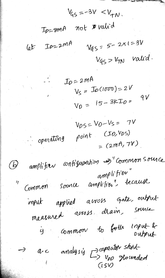
2. The MOSFET in the amplifier below has a threshold voltage of IV and a transconductance parameter of ImA/V a) Estimate the operating point of the transistor. b) Sketch the small-signal model and de...
Rsig Nahyan vgs ( gmugs, r01 RDS Vsig ) Ril Consider the small signal equivalent circuit...
 Rsig Nahyan vgs ( gmugs, r01 RDS Vsig ) Ril Consider the small signal equivalent circuit of an amplifier shown above. The parameters are given to be: R1 = 3000, R2 = 10160, R2=100%, RD=RL=50 Rsig = 202, VGS1=3.5V. Vt = 0.5V and kn = 1mA/V^2. The transistor output resistances are represented by ro1, ra2 with both the transistors in saturation and having |MAL= 40V and same DC current flowing through them Find the small signal parameter of the MOSFET:...
A common source amplifier circuit based on a single n-channel MOSFET is shown in Figure 4b. Assume that the transconductance gm-60 mS (equivalent to mA/ V) and drain source resistance, os,...
 A common source amplifier circuit based on a single n-channel MOSFET is shown in Figure 4b. Assume that the transconductance gm-60 mS (equivalent to mA/ V) and drain source resistance, os, is so large it may be neglected. 0) Calculate the open circuit voltage gain Av Yout/ Vis. i) The amplifier has a load of 10 k2. Determine the current gain Va. = 12 V 150k 4k3 Vout Vin 200k GND = 0 V Figure 4b a) State the name...
Problem #5 (20 points) n the two stage cascade amplifier circuit shown below, the MOSFET has...
 Problem #5 (20 points) n the two stage cascade amplifier circuit shown below, the MOSFET has V IV and k-0s mA/ and the BIT has p 100 a) Perform the DC analysis of this circuit and based on the appropriate DC current values, calculate the small signal parameters for each transistor. b) Replace each transistor with its appropriate small signal model (neglecting ro) and draw the resulting smali- signal circuit for this amplifier circuit. HINT: You may use the T-model...
The circuit below is a common collector (CC) circuit. Assuming VBEON VA, and ß - 100, , VCE.SAT 0.2V, VA 00 Calculate the transistor operating point. a. 1 b. Find the small signal voltage gain, 。 Fi...
 The circuit below is a common collector (CC) circuit.
Assuming VBEON VA, and ß - 100, , VCE.SAT 0.2V, VA 00 Calculate the transistor operating point. a. 1 b. Find the small signal voltage gain, 。 Find the driving point input resistance. c. d. If the input is a sinewave, find the maximum output voltage amplitude before clıpping sets in. B1 CO Q1 RE v,RB2
Assuming VBEON VA, and ß - 100, , VCE.SAT 0.2V, VA 00 Calculate the transistor...
The circuit below is a common collector (CC) circuit.
Assuming VBEON VA, and ß - 100, , VCE.SAT 0.2V, VA 00 Calculate the transistor operating point. a. 1 b. Find the small signal voltage gain, 。 Find the driving point input resistance. c. d. If the input is a sinewave, find the maximum output voltage amplitude before clıpping sets in. B1 CO Q1 RE v,RB2
Assuming VBEON VA, and ß - 100, , VCE.SAT 0.2V, VA 00 Calculate the transistor...
*Note : MOSFET-2N7002 Parameter => Vt : 1.47V, kn = 0.048 A/V^2 1. Obtain [ the...
 *Note : MOSFET-2N7002 Parameter => Vt : 1.47V, kn = 0.048
A/V^2
1. Obtain [ the Voltage and current ] of [ each node and branch
] at DC bias point (operating point) in the common-source +
source-follower figure above.
2. Obtain the small-signal equivalent model of the figure above
at DC bias point , then obtain open-circuit voltage gain Avo, input
resistance Rin, output resistance Rout.
tran 0 100m 99m 0.001m ;op 0 100m 99m 0.001m VDD V1 +...
*Note : MOSFET-2N7002 Parameter => Vt : 1.47V, kn = 0.048
A/V^2
1. Obtain [ the Voltage and current ] of [ each node and branch
] at DC bias point (operating point) in the common-source +
source-follower figure above.
2. Obtain the small-signal equivalent model of the figure above
at DC bias point , then obtain open-circuit voltage gain Avo, input
resistance Rin, output resistance Rout.
tran 0 100m 99m 0.001m ;op 0 100m 99m 0.001m VDD V1 +...
Problem 3: Design Problem On Figure P3a, you have a Common Source (CS) n-channel MOSFET amplifier....
 Problem 3: Design Problem On Figure P3a, you have a Common Source (CS) n-channel MOSFET amplifier. Notice the absence of a source resistor Rsig and load resistor R. If we know how the present amplifier (the one on Figure P3a) behaves without Rsig and RL, we can infer its behaviors if Rsig and R were to be added. design the amplifier circuit on Figure P3a, i.e., you have to find appropriate values for RGj You are to RG,, RD, and...
 Rsig Nahyan vgs ( gmugs, r01 RDS Vsig ) Ril Consider the small signal equivalent circuit of an amplifier shown above. The parameters are given to be: R1 = 3000, R2 = 10160, R2=100%, RD=RL=50 Rsig = 202, VGS1=3.5V. Vt = 0.5V and kn = 1mA/V^2. The transistor output resistances are represented by ro1, ra2 with both the transistors in saturation and having |MAL= 40V and same DC current flowing through them Find the small signal parameter of the MOSFET:...
 A common source amplifier circuit based on a single n-channel MOSFET is shown in Figure 4b. Assume that the transconductance gm-60 mS (equivalent to mA/ V) and drain source resistance, os, is so large it may be neglected. 0) Calculate the open circuit voltage gain Av Yout/ Vis. i) The amplifier has a load of 10 k2. Determine the current gain Va. = 12 V 150k 4k3 Vout Vin 200k GND = 0 V Figure 4b a) State the name...
 Problem #5 (20 points) n the two stage cascade amplifier circuit shown below, the MOSFET has V IV and k-0s mA/ and the BIT has p 100 a) Perform the DC analysis of this circuit and based on the appropriate DC current values, calculate the small signal parameters for each transistor. b) Replace each transistor with its appropriate small signal model (neglecting ro) and draw the resulting smali- signal circuit for this amplifier circuit. HINT: You may use the T-model...
 The circuit below is a common collector (CC) circuit.
Assuming VBEON VA, and ß - 100, , VCE.SAT 0.2V, VA 00 Calculate the transistor operating point. a. 1 b. Find the small signal voltage gain, 。 Find the driving point input resistance. c. d. If the input is a sinewave, find the maximum output voltage amplitude before clıpping sets in. B1 CO Q1 RE v,RB2
Assuming VBEON VA, and ß - 100, , VCE.SAT 0.2V, VA 00 Calculate the transistor...
The circuit below is a common collector (CC) circuit.
Assuming VBEON VA, and ß - 100, , VCE.SAT 0.2V, VA 00 Calculate the transistor operating point. a. 1 b. Find the small signal voltage gain, 。 Find the driving point input resistance. c. d. If the input is a sinewave, find the maximum output voltage amplitude before clıpping sets in. B1 CO Q1 RE v,RB2
Assuming VBEON VA, and ß - 100, , VCE.SAT 0.2V, VA 00 Calculate the transistor...
 *Note : MOSFET-2N7002 Parameter => Vt : 1.47V, kn = 0.048
A/V^2
1. Obtain [ the Voltage and current ] of [ each node and branch
] at DC bias point (operating point) in the common-source +
source-follower figure above.
2. Obtain the small-signal equivalent model of the figure above
at DC bias point , then obtain open-circuit voltage gain Avo, input
resistance Rin, output resistance Rout.
tran 0 100m 99m 0.001m ;op 0 100m 99m 0.001m VDD V1 +...
*Note : MOSFET-2N7002 Parameter => Vt : 1.47V, kn = 0.048
A/V^2
1. Obtain [ the Voltage and current ] of [ each node and branch
] at DC bias point (operating point) in the common-source +
source-follower figure above.
2. Obtain the small-signal equivalent model of the figure above
at DC bias point , then obtain open-circuit voltage gain Avo, input
resistance Rin, output resistance Rout.
tran 0 100m 99m 0.001m ;op 0 100m 99m 0.001m VDD V1 +...
 Problem 3: Design Problem On Figure P3a, you have a Common Source (CS) n-channel MOSFET amplifier. Notice the absence of a source resistor Rsig and load resistor R. If we know how the present amplifier (the one on Figure P3a) behaves without Rsig and RL, we can infer its behaviors if Rsig and R were to be added. design the amplifier circuit on Figure P3a, i.e., you have to find appropriate values for RGj You are to RG,, RD, and...
Most questions answered within 3 hours.
-
Where is the error in this code sequence?
String s1 = "Hello";
String s2 = "ello";...
asked 11 months ago -
Financial data for Joel de Paris, Inc., for last year
follow:
Joel de Paris, Inc.
Balance...
asked 11 months ago -
Consider this reaction:
Al2(SO4)3 (aq)+ BaCl3
(aq) Al2Cl6 (aq)- +
3BaSO4(s) . What is the...
asked 11 months ago -
Suppose that Savneet is considering increasing her
recent random sample from 20 car rentals to 40...
asked 11 months ago -
Trucks arrive at an unloading terminal at an average rate of 120
per hour.
Trucks arrive...
asked 11 months ago -
Why are methanol and ethanol completely soluble in water while
octanol is not very little soluble....
asked 11 months ago -
A facilities manager at a university reads in a research report
that the mean amount of...
asked 11 months ago -
When the CuSO4 is rehydrated by adding water to the anhydrous
compound, is this an endothermic...
asked 11 months ago -
A ray of sunlight is passing from diamond into crown glass; the
angle of incidence is...
asked 11 months ago -
A block of mass 0.249 kg is placed on top of a light, vertical
spring of...
asked 11 months ago -
how do the kidneys compensate in the presences of acidosis
a) trigger hyperventilate
b) reserve acid...
asked 11 months ago -
Question 501 pts
The rental rate of capital to the firm increases. Which of the
following...
asked 11 months ago