
Homework Answers
Add Answer to:
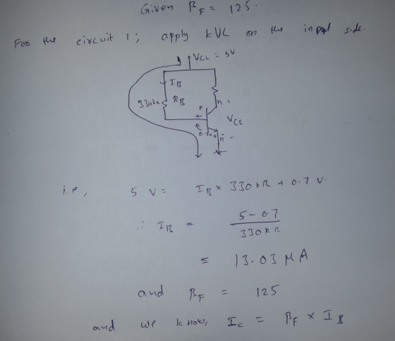
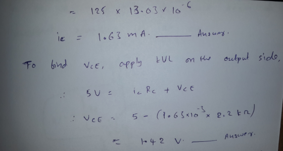
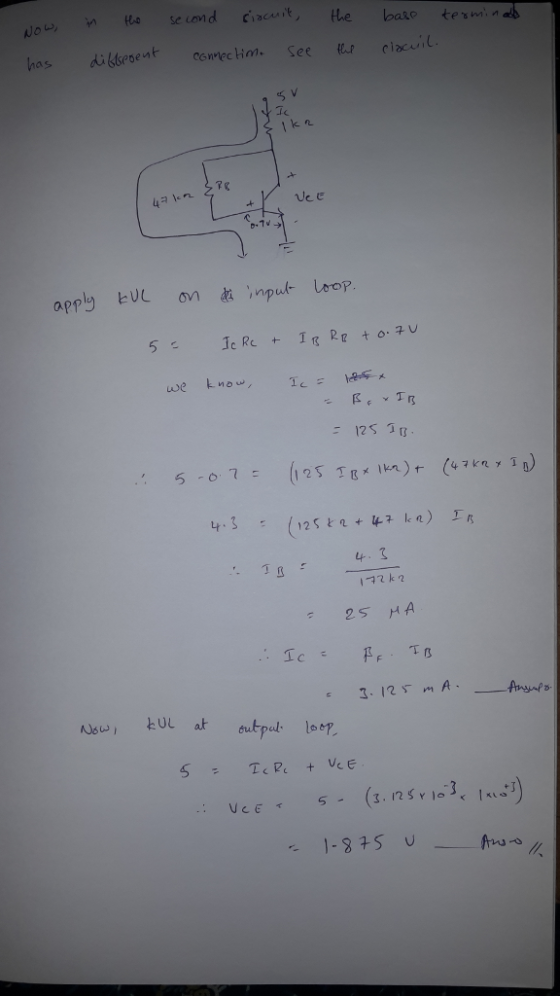
For each of the NPN transistor circuits shown, calculate ic and vcE. The NPNs both have...
1. For the npn transistor shown in Fig. 1, assue a 98/99, V)0.7V and VCE(sal) 0.2V....
 1. For the npn transistor shown in Fig. 1, assue a 98/99, V)0.7V and VCE(sal) 0.2V. Plot Voul, lc, IE ald Ic/IB as a function of IB for 0 < 1B < 150??. 10V 1k Figure 1
draw a (simplified) schematic !! An npn transistor having IS-10-15A and β = 100 is connected shown. Assuming the transistor is in active mode, find VBE and VCE. 10μΑ Draw a schematic for this mode...
 draw a (simplified) schematic !!
An npn transistor having IS-10-15A and β = 100 is connected shown. Assuming the transistor is in active mode, find VBE and VCE. 10μΑ Draw a schematic for this model! CE
An npn transistor having IS-10-15A and β = 100 is connected shown. Assuming the transistor is in active mode, find VBE and VCE. 10μΑ Draw a schematic for this model! CE
draw a (simplified) schematic !!
An npn transistor having IS-10-15A and β = 100 is connected shown. Assuming the transistor is in active mode, find VBE and VCE. 10μΑ Draw a schematic for this model! CE
An npn transistor having IS-10-15A and β = 100 is connected shown. Assuming the transistor is in active mode, find VBE and VCE. 10μΑ Draw a schematic for this model! CE
3. For the circuit shown a. Determine the levels of IB, Ic and Vce for the...
 3. For the circuit shown a. Determine the levels of IB, Ic and Vce for the circuit shown. b. Change B to 150 (36.4% increase), and calculate the new levels of IB, Ic and VCE. c. Determine the magnitude of the percentage change in Ic and VCE +24 V 470 k 2 B = 110
Vcc 10 V #2. Calculate the values of VBE, VCE, IB, Ic, and IE assuming B...
 Vcc 10 V #2. Calculate the values of VBE, VCE, IB, Ic, and IE assuming B = 150 for the Transistor Biasing Circuit in Figure 5 - 5. Simulate the circuit in Figure 5 - 5. Include the procedure and results of calculation / simulation in related section. 370k SR2 2370K BROD 2N3904 ŽR3 330 Figure 5 -5: Transistor Biasing
4. Determine the terminal voltages of each transistor with respect to ground for each circuit in ...
 4. Determine the terminal voltages of each transistor with respect to ground for each circuit in the Figure shown. Also determine VcE. VBe, and VcB- Ans: Vc=-12 V Vy--4V VBE =-0.7 V ½ =-3.3 V Va. =-8.7 V 4 V RE 2.2 kΩ CE
4. Determine the terminal voltages of each transistor with respect to ground for each circuit in the Figure shown. Also determine VcE. VBe, and VcB- Ans: Vc=-12 V Vy--4V VBE =-0.7 V ½ =-3.3 V Va....
4. Determine the terminal voltages of each transistor with respect to ground for each circuit in the Figure shown. Also determine VcE. VBe, and VcB- Ans: Vc=-12 V Vy--4V VBE =-0.7 V ½ =-3.3 V Va. =-8.7 V 4 V RE 2.2 kΩ CE
4. Determine the terminal voltages of each transistor with respect to ground for each circuit in the Figure shown. Also determine VcE. VBe, and VcB- Ans: Vc=-12 V Vy--4V VBE =-0.7 V ½ =-3.3 V Va....
Consider the npn BJT with a turn-on voltage V1 = 0.70 V, and a saturation emitter-collector...
 Consider the npn BJT with a turn-on voltage V1 = 0.70 V, and a saturation emitter-collector voltage V CE/SAT) = 0.20 V. (a) [20 points) Consider this transistor in a common- emitter circuit (Re = 0). Design this common- emitter circuit to produce the IV (Ic vs. VCE) characteristic and load line (LL) as shown in the graph. Your answers are the following: a drawing of the circuit; the values of Vcc, Rc, VBB, and Ra; and the value for...
1. For the transistor circuit shown in figure 1, what is: a. Vce when VIN =...
 1. For the transistor circuit shown in figure 1, what is: a. Vce when VIN = OV? b. What minimum value of IB is required to saturate the transistor if Boc is 200? c. Calculate the maximum value of Rs when Vin = 5V. VCC 10V RC 1.0 K RB Q1 VIN=0V 15C02MH-TLE GND Figure
The NPN transistor in the circuit shown haes B-60 Assuming that the BJT is operating in the deep ...
 answer i-iv please
The NPN transistor in the circuit shown haes B-60 Assuming that the BJT is operating in the deep saturation mode ie. VCEsat-02y and VBE-07V ßforced-10. Question 3: 20% p-60) Assuming that the BJT is operating in the deep Rg i) Calculate collector current, Ic. (4%) ii) Calculate voltage VBB and base current,IB(6%) iii) If we keep VBB and Rc the same, i.e. at 1k2, what is the minimum value of RB to restore the transistor beta to...
answer i-iv please
The NPN transistor in the circuit shown haes B-60 Assuming that the BJT is operating in the deep saturation mode ie. VCEsat-02y and VBE-07V ßforced-10. Question 3: 20% p-60) Assuming that the BJT is operating in the deep Rg i) Calculate collector current, Ic. (4%) ii) Calculate voltage VBB and base current,IB(6%) iii) If we keep VBB and Rc the same, i.e. at 1k2, what is the minimum value of RB to restore the transistor beta to...
7. Determine the quiescent levels of Ic and Vce for the network of Figure 25. 10...
 7. Determine the quiescent levels of Ic and Vce for the network of Figure 25. 10 V 4.7 k92 250 k22 16 10 uF B = 90 OH 10 uF 1.2 ΚΩ Figure 25 8. A stage is a transistor and the passive components connected to it. Figure 26 shows a three-stage circuit using two-supply emitter bias. Vec +15 V RCI 10 ΚΩ Ro 10 ΚΩ Rc 10 k 2 Yout R1 RB3 w- RER 33 k22 33 k2 RE1...
What type of transistor amplifier is shown in Fig. 29-19a? 29-3 +Vcc 15 V = 7.5...
 What type of transistor amplifier is shown in Fig. 29-19a? 29-3 +Vcc 15 V = 7.5 k R= 1.2 k R, C B= 100 2 = 1.5 k° in 10 mV RE = 360 CE (a) Calculate the following DC quantities in Fig. 29-19a: 29-4 Ves a. b. VE C. d. Vc e. VCE W
What type of transistor amplifier is shown in Fig. 29-19a? 29-3 +Vcc 15 V = 7.5 k R= 1.2 k R, C B= 100 2...
What type of transistor amplifier is shown in Fig. 29-19a? 29-3 +Vcc 15 V = 7.5 k R= 1.2 k R, C B= 100 2 = 1.5 k° in 10 mV RE = 360 CE (a) Calculate the following DC quantities in Fig. 29-19a: 29-4 Ves a. b. VE C. d. Vc e. VCE W
What type of transistor amplifier is shown in Fig. 29-19a? 29-3 +Vcc 15 V = 7.5 k R= 1.2 k R, C B= 100 2...
 1. For the npn transistor shown in Fig. 1, assue a 98/99, V)0.7V and VCE(sal) 0.2V. Plot Voul, lc, IE ald Ic/IB as a function of IB for 0 < 1B < 150??. 10V 1k Figure 1
 draw a (simplified) schematic !!
An npn transistor having IS-10-15A and β = 100 is connected shown. Assuming the transistor is in active mode, find VBE and VCE. 10μΑ Draw a schematic for this model! CE
An npn transistor having IS-10-15A and β = 100 is connected shown. Assuming the transistor is in active mode, find VBE and VCE. 10μΑ Draw a schematic for this model! CE
draw a (simplified) schematic !!
An npn transistor having IS-10-15A and β = 100 is connected shown. Assuming the transistor is in active mode, find VBE and VCE. 10μΑ Draw a schematic for this model! CE
An npn transistor having IS-10-15A and β = 100 is connected shown. Assuming the transistor is in active mode, find VBE and VCE. 10μΑ Draw a schematic for this model! CE
 3. For the circuit shown a. Determine the levels of IB, Ic and Vce for the circuit shown. b. Change B to 150 (36.4% increase), and calculate the new levels of IB, Ic and VCE. c. Determine the magnitude of the percentage change in Ic and VCE +24 V 470 k 2 B = 110
 Vcc 10 V #2. Calculate the values of VBE, VCE, IB, Ic, and IE assuming B = 150 for the Transistor Biasing Circuit in Figure 5 - 5. Simulate the circuit in Figure 5 - 5. Include the procedure and results of calculation / simulation in related section. 370k SR2 2370K BROD 2N3904 ŽR3 330 Figure 5 -5: Transistor Biasing
 4. Determine the terminal voltages of each transistor with respect to ground for each circuit in the Figure shown. Also determine VcE. VBe, and VcB- Ans: Vc=-12 V Vy--4V VBE =-0.7 V ½ =-3.3 V Va. =-8.7 V 4 V RE 2.2 kΩ CE
4. Determine the terminal voltages of each transistor with respect to ground for each circuit in the Figure shown. Also determine VcE. VBe, and VcB- Ans: Vc=-12 V Vy--4V VBE =-0.7 V ½ =-3.3 V Va....
4. Determine the terminal voltages of each transistor with respect to ground for each circuit in the Figure shown. Also determine VcE. VBe, and VcB- Ans: Vc=-12 V Vy--4V VBE =-0.7 V ½ =-3.3 V Va. =-8.7 V 4 V RE 2.2 kΩ CE
4. Determine the terminal voltages of each transistor with respect to ground for each circuit in the Figure shown. Also determine VcE. VBe, and VcB- Ans: Vc=-12 V Vy--4V VBE =-0.7 V ½ =-3.3 V Va....
 Consider the npn BJT with a turn-on voltage V1 = 0.70 V, and a saturation emitter-collector voltage V CE/SAT) = 0.20 V. (a) [20 points) Consider this transistor in a common- emitter circuit (Re = 0). Design this common- emitter circuit to produce the IV (Ic vs. VCE) characteristic and load line (LL) as shown in the graph. Your answers are the following: a drawing of the circuit; the values of Vcc, Rc, VBB, and Ra; and the value for...
 1. For the transistor circuit shown in figure 1, what is: a. Vce when VIN = OV? b. What minimum value of IB is required to saturate the transistor if Boc is 200? c. Calculate the maximum value of Rs when Vin = 5V. VCC 10V RC 1.0 K RB Q1 VIN=0V 15C02MH-TLE GND Figure
 answer i-iv please
The NPN transistor in the circuit shown haes B-60 Assuming that the BJT is operating in the deep saturation mode ie. VCEsat-02y and VBE-07V ßforced-10. Question 3: 20% p-60) Assuming that the BJT is operating in the deep Rg i) Calculate collector current, Ic. (4%) ii) Calculate voltage VBB and base current,IB(6%) iii) If we keep VBB and Rc the same, i.e. at 1k2, what is the minimum value of RB to restore the transistor beta to...
answer i-iv please
The NPN transistor in the circuit shown haes B-60 Assuming that the BJT is operating in the deep saturation mode ie. VCEsat-02y and VBE-07V ßforced-10. Question 3: 20% p-60) Assuming that the BJT is operating in the deep Rg i) Calculate collector current, Ic. (4%) ii) Calculate voltage VBB and base current,IB(6%) iii) If we keep VBB and Rc the same, i.e. at 1k2, what is the minimum value of RB to restore the transistor beta to...
 7. Determine the quiescent levels of Ic and Vce for the network of Figure 25. 10 V 4.7 k92 250 k22 16 10 uF B = 90 OH 10 uF 1.2 ΚΩ Figure 25 8. A stage is a transistor and the passive components connected to it. Figure 26 shows a three-stage circuit using two-supply emitter bias. Vec +15 V RCI 10 ΚΩ Ro 10 ΚΩ Rc 10 k 2 Yout R1 RB3 w- RER 33 k22 33 k2 RE1...
 What type of transistor amplifier is shown in Fig. 29-19a? 29-3 +Vcc 15 V = 7.5 k R= 1.2 k R, C B= 100 2 = 1.5 k° in 10 mV RE = 360 CE (a) Calculate the following DC quantities in Fig. 29-19a: 29-4 Ves a. b. VE C. d. Vc e. VCE W
What type of transistor amplifier is shown in Fig. 29-19a? 29-3 +Vcc 15 V = 7.5 k R= 1.2 k R, C B= 100 2...
What type of transistor amplifier is shown in Fig. 29-19a? 29-3 +Vcc 15 V = 7.5 k R= 1.2 k R, C B= 100 2 = 1.5 k° in 10 mV RE = 360 CE (a) Calculate the following DC quantities in Fig. 29-19a: 29-4 Ves a. b. VE C. d. Vc e. VCE W
What type of transistor amplifier is shown in Fig. 29-19a? 29-3 +Vcc 15 V = 7.5 k R= 1.2 k R, C B= 100 2...
Most questions answered within 3 hours.
-
Where is the error in this code sequence?
String s1 = "Hello";
String s2 = "ello";...
asked 11 months ago -
Financial data for Joel de Paris, Inc., for last year
follow:
Joel de Paris, Inc.
Balance...
asked 11 months ago -
Consider this reaction:
Al2(SO4)3 (aq)+ BaCl3
(aq) Al2Cl6 (aq)- +
3BaSO4(s) . What is the...
asked 11 months ago -
Suppose that Savneet is considering increasing her
recent random sample from 20 car rentals to 40...
asked 11 months ago -
Trucks arrive at an unloading terminal at an average rate of 120
per hour.
Trucks arrive...
asked 11 months ago -
Why are methanol and ethanol completely soluble in water while
octanol is not very little soluble....
asked 11 months ago -
A facilities manager at a university reads in a research report
that the mean amount of...
asked 11 months ago -
When the CuSO4 is rehydrated by adding water to the anhydrous
compound, is this an endothermic...
asked 11 months ago -
A ray of sunlight is passing from diamond into crown glass; the
angle of incidence is...
asked 11 months ago -
A block of mass 0.249 kg is placed on top of a light, vertical
spring of...
asked 11 months ago -
how do the kidneys compensate in the presences of acidosis
a) trigger hyperventilate
b) reserve acid...
asked 11 months ago -
Question 501 pts
The rental rate of capital to the firm increases. Which of the
following...
asked 11 months ago