
Homework Answers
Add Answer to:
(b) A structure that we sometimes encounter in electronic devices is a so-called p-i-n structure, consisting...
(b) A structure that we sometimes encounter in electronic devices is a so-called p-i-n structure, consisting...
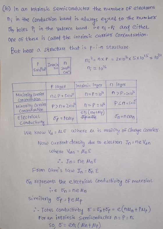
 (b) A structure that we sometimes encounter in electronic devices is a so-called p-i-n structure, consisting of a p-doped layer, an intrinsic layer and then an n-doped layer as shown in the drawing below. Assume Si as the semiconductor: Ps. Intrinsic n kx10cn' 5XIOCA p layer Intrinsic layer n layer Majority carrier concentration Minority carrier concentration Electrical Conductivity
(iv) Explain what process(es) will be different at the higher temperature producing the different features from...
 (iv) Explain what process(es) will be different at the higher temperature producing the different features from (ii) to (iii). (2) (b) A structure that we sometimes encounter in electronic devices is a so-called p-i-n structure, consisting of a p-doped layer, an intrinsic layer and then an n-doped layer as shown in the drawing below. Assume Si as the semiconductor: P US- [Intrinsic 5 XION n kx 10 cm Assume a temperature of 300 K and with the doping as indicated...
solid state electronic devices ch5 pro22 In a simple p-n diode, if the diffusion coefficent for...
 solid state electronic devices ch5 pro22
In a simple p-n diode, if the diffusion coefficent for holes is twice than that for the electrons, the minority carrier concentration at n side is twice than that in p side, and the diffusion coefficent for holes is also twice of that for the electrons, calculate the injection efficiency for this diode at x, = 0.
solid state electronic devices ch5 pro22
In a simple p-n diode, if the diffusion coefficent for holes is twice than that for the electrons, the minority carrier concentration at n side is twice than that in p side, and the diffusion coefficent for holes is also twice of that for the electrons, calculate the injection efficiency for this diode at x, = 0.
Taking pure silicon (Si) as an example, explain what is meant by the terms electron-hole generation...
 Taking pure silicon (Si) as an example, explain what is meant by the terms electron-hole generation and recombination, how they affect the electrical conductivity, and define what is meant by the "intrinsic carrier density", n. [5 marks] Q3. a) b) With the aid of both lattice and energy band diagrams, explain how n-type doping of Si is achieved and state two types of suitable dopant atoms. [7 marks] c) An n-type region on a Si wafer has a donor concentration...
B2 Consider a diode formed by making a p-n junction structure in a silicon sample as shown in Fig. B2. nt laver p-type...
 B2 Consider a diode formed by making a p-n junction structure in a silicon sample as shown in Fig. B2. nt laver p-type Si Fig. B2 (a). If the dopant concentrations of the n layer and the p-type silicon are 6x101" cm and 8x10 cm respectively, calculate the built-in potential of the p-n junction at room temperature (300 K) 15 (3 marks) (b). Due to overheating of the silicon sample, the diode has an operation temperature of 200 °C and...
Please help me out.. Need to pass this course as a removal for my other course.....
 Please help me out.. Need to pass this course as a removal for
my other course..
Si material parameters: Band gap energy at 300 K: Eg = 1.124 eV Relative permittivity: x = 11.7 Effective mass of electron: m =1.08m for density of states, Effective mass of hole: m = 0.81m for density of states, m = 0.26m for conductivity m =0.39m for conductivity Up = 470 cm/V.s Mobility: Un = 1400 cm /V-s, Diffusion coefficient: Do = 36 cm²/s,...
Please help me out.. Need to pass this course as a removal for
my other course..
Si material parameters: Band gap energy at 300 K: Eg = 1.124 eV Relative permittivity: x = 11.7 Effective mass of electron: m =1.08m for density of states, Effective mass of hole: m = 0.81m for density of states, m = 0.26m for conductivity m =0.39m for conductivity Up = 470 cm/V.s Mobility: Un = 1400 cm /V-s, Diffusion coefficient: Do = 36 cm²/s,...
 (b) A structure that we sometimes encounter in electronic devices is a so-called p-i-n structure, consisting of a p-doped layer, an intrinsic layer and then an n-doped layer as shown in the drawing below. Assume Si as the semiconductor: Ps. Intrinsic n kx10cn' 5XIOCA p layer Intrinsic layer n layer Majority carrier concentration Minority carrier concentration Electrical Conductivity
 (iv) Explain what process(es) will be different at the higher temperature producing the different features from (ii) to (iii). (2) (b) A structure that we sometimes encounter in electronic devices is a so-called p-i-n structure, consisting of a p-doped layer, an intrinsic layer and then an n-doped layer as shown in the drawing below. Assume Si as the semiconductor: P US- [Intrinsic 5 XION n kx 10 cm Assume a temperature of 300 K and with the doping as indicated...
 solid state electronic devices ch5 pro22
In a simple p-n diode, if the diffusion coefficent for holes is twice than that for the electrons, the minority carrier concentration at n side is twice than that in p side, and the diffusion coefficent for holes is also twice of that for the electrons, calculate the injection efficiency for this diode at x, = 0.
solid state electronic devices ch5 pro22
In a simple p-n diode, if the diffusion coefficent for holes is twice than that for the electrons, the minority carrier concentration at n side is twice than that in p side, and the diffusion coefficent for holes is also twice of that for the electrons, calculate the injection efficiency for this diode at x, = 0.
 Taking pure silicon (Si) as an example, explain what is meant by the terms electron-hole generation and recombination, how they affect the electrical conductivity, and define what is meant by the "intrinsic carrier density", n. [5 marks] Q3. a) b) With the aid of both lattice and energy band diagrams, explain how n-type doping of Si is achieved and state two types of suitable dopant atoms. [7 marks] c) An n-type region on a Si wafer has a donor concentration...
 B2 Consider a diode formed by making a p-n junction structure in a silicon sample as shown in Fig. B2. nt laver p-type Si Fig. B2 (a). If the dopant concentrations of the n layer and the p-type silicon are 6x101" cm and 8x10 cm respectively, calculate the built-in potential of the p-n junction at room temperature (300 K) 15 (3 marks) (b). Due to overheating of the silicon sample, the diode has an operation temperature of 200 °C and...
 Please help me out.. Need to pass this course as a removal for
my other course..
Si material parameters: Band gap energy at 300 K: Eg = 1.124 eV Relative permittivity: x = 11.7 Effective mass of electron: m =1.08m for density of states, Effective mass of hole: m = 0.81m for density of states, m = 0.26m for conductivity m =0.39m for conductivity Up = 470 cm/V.s Mobility: Un = 1400 cm /V-s, Diffusion coefficient: Do = 36 cm²/s,...
Please help me out.. Need to pass this course as a removal for
my other course..
Si material parameters: Band gap energy at 300 K: Eg = 1.124 eV Relative permittivity: x = 11.7 Effective mass of electron: m =1.08m for density of states, Effective mass of hole: m = 0.81m for density of states, m = 0.26m for conductivity m =0.39m for conductivity Up = 470 cm/V.s Mobility: Un = 1400 cm /V-s, Diffusion coefficient: Do = 36 cm²/s,...
Most questions answered within 3 hours.
-
Where is the error in this code sequence?
String s1 = "Hello";
String s2 = "ello";...
asked 10 months ago -
Financial data for Joel de Paris, Inc., for last year
follow:
Joel de Paris, Inc.
Balance...
asked 10 months ago -
Consider this reaction:
Al2(SO4)3 (aq)+ BaCl3
(aq) Al2Cl6 (aq)- +
3BaSO4(s) . What is the...
asked 10 months ago -
Suppose that Savneet is considering increasing her
recent random sample from 20 car rentals to 40...
asked 10 months ago -
Trucks arrive at an unloading terminal at an average rate of 120
per hour.
Trucks arrive...
asked 10 months ago -
Why are methanol and ethanol completely soluble in water while
octanol is not very little soluble....
asked 10 months ago -
A facilities manager at a university reads in a research report
that the mean amount of...
asked 10 months ago -
When the CuSO4 is rehydrated by adding water to the anhydrous
compound, is this an endothermic...
asked 10 months ago -
A ray of sunlight is passing from diamond into crown glass; the
angle of incidence is...
asked 10 months ago -
A block of mass 0.249 kg is placed on top of a light, vertical
spring of...
asked 10 months ago -
how do the kidneys compensate in the presences of acidosis
a) trigger hyperventilate
b) reserve acid...
asked 10 months ago -
Question 501 pts
The rental rate of capital to the firm increases. Which of the
following...
asked 10 months ago