
Homework Answers

Add Answer to:
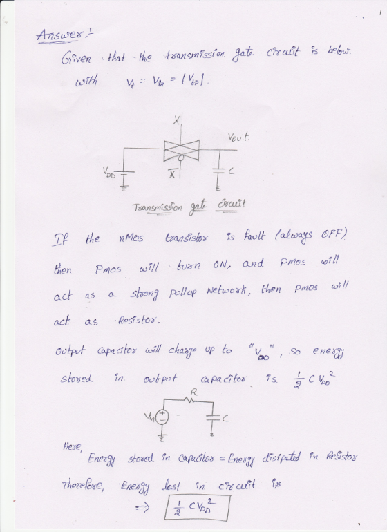
Fig. 3 with V Vnp.Assume Consider the transmission gate circuit shown in that VouT 0V at...
Problem 1 -Integrated Common Source Amplifier: For the circuit in Fig.1, draw the small signal equivalent...
 Problem 1 -Integrated Common Source Amplifier: For the circuit in Fig.1, draw the small signal equivalent circuit and find the following small signal values: gm1 go1 go2 Vout/Vin Rout You can assume that the overdrive voltage for all transistors is 0.2V and A for the NMOS and PMOS are 0.1V1 and 0.05V1 respectively. The drain source current of the transistors M1 and M2 is 20HA. All gate lengths of homework 3.) 0.5um. (The DC analysis for this circuit was done...
A21921 2. +9V Re Vout Re RE CE 0v Figure 3 (a) ) State the purpose of each of the capacitors Cin, Cout and Ce in the circuit [3 shown in Figure 3. (i) Derive an expression for the input resistanc...
 A21921 2. +9V Re Vout Re RE CE 0v Figure 3 (a) ) State the purpose of each of the capacitors Cin, Cout and Ce in the circuit [3 shown in Figure 3. (i) Derive an expression for the input resistance of this circuit in terms of the [5 mutual conductance of the transistor gm and its current gain β. we require an amplifier with a gain of-100, an output impedance of 1kΩ and an input impedance of 1k2. The...
4) For all 3 examples convert the minimized Boolean equation into (a) Gate circuit diagram (i.e....
 4) For all 3 examples convert the minimized Boolean equation into (a) Gate circuit diagram (i.e. AND, OR, NOR, NAND, XOR, NOT, XNOR etc.) (b) Transistor circuit diagram (i.e. NMOS, PMOS) АВС Yi Y O0 0 0 0 1 0 1 0 0 1 0 1 1 0 1 1 1 1 00 0 0 0 1 0 1 1 10 0 1 1 1 0 Equations for the truth table given be p, and the rows for (c,d), i.e.,...
3. For the circuit below in ouut assume that at t-0, Vin 0V and that there...
 3. For the circuit below in ouut assume that at t-0, Vin 0V and that there is no charge on either of the capacitors Show that for all later times and derive an expression for G in terms of Ci and C2 We'll discuss in class the circumstances in which it might make sense to design a circuit like this using capacitors instead of resistors.
8.38. For Fig. 8.63, analyze the functionality of circuit and derive expression for Vout. 2. For...
 8.38. For Fig. 8.63, analyze the functionality of circuit and
derive expression for Vout.
2. For Fig.8.66(a cir- for the input cuit and verify its function mathematically.the current mior a func- 8.37.For AA.S Vin2 oltage 2 k wollol od M1 C MoHomout + Vin1 C OT + Wcg ab sub vo taum coo o ni TOTI9 9283-1210w ort nbFigure 8.62 or bns .0 wolod nism TIT smon&i 8.38. For Fig. 8.63, analyze the functionality of mcircuit and derive expression for...
8.38. For Fig. 8.63, analyze the functionality of circuit and
derive expression for Vout.
2. For Fig.8.66(a cir- for the input cuit and verify its function mathematically.the current mior a func- 8.37.For AA.S Vin2 oltage 2 k wollol od M1 C MoHomout + Vin1 C OT + Wcg ab sub vo taum coo o ni TOTI9 9283-1210w ort nbFigure 8.62 or bns .0 wolod nism TIT smon&i 8.38. For Fig. 8.63, analyze the functionality of mcircuit and derive expression for...
An analogue amplifier circuit is shown in Figure 1 below. VDD Q5 15V JL - Vout...
 An analogue amplifier circuit is shown in Figure 1 below. VDD Q5 15V JL - Vout Irer RI Vina JET T7T Figure 1 Integrated amplifier circuit. Circuit Data: Vpp = 15 V, IREF = I1 = I2 = 1.0 mA Transistor Data: Q1: NMOS, un Cox = 80 A/V?, W/L = 100 um/0.8 um, Vtn = 0.8 V, L = 0.10 um/V Q2: NPN BJT, B = 100, Vbe = 0.7 V, VA = 150 V Q3, Q4: NMOS, un...
Fig. 3 as follows is an IC layout of a CMOS implementation of a two-input digital...
 Fig. 3 as follows is an IC layout of a CMOS implementation of a two-input digital logic gate. The truth table of the logic gate is also given. Voo Vini Vina Vout OVOV 3 V OV 3V 3 V Vint Vina out 3V10 V 3V 3V 3V OV GND Fig. 3 (a). How many MOSFETs are there in the IC layout shown above? (2 marks) (b). The given layout is drawn according to the lambda () design rules. If a...
(a) The circuit shown below in Figure 3 has a two-input logic gate hidden from view....
 (a) The circuit shown below in Figure 3 has a two-input logic gate hidden from view. By inspection of the output function F, identify the hidden logic gate. ; hidden logic F-(ADB)(C08) gate cas Figure 3 (b) Draw a truth table for the function F given in part (a) above and hence derive an alternative 'sum of products' expression for F.
Q4- A circuit diagram of a forward converter is shown in Fig. 3. V-200V, Vout-5V, fs= 100kHz, nún,-5, Lm-15m H, L=0.05...
 Q4- A circuit diagram of a forward converter is shown in Fig. 3. V-200V, Vout-5V, fs= 100kHz, nún,-5, Lm-15m H, L=0.05mH. (a) Find the maximum value of duty cycle. (b) If the duty cycle is 0.5, find the turns ratio ni:nz. (c) If n n is as calculated in (b), what is the lowest input voltage allowed if Vout is to be kept equal to 5V? D, n, n, A/ D3 O1 Fig. 3.
Q4- A circuit diagram of a...
Q4- A circuit diagram of a forward converter is shown in Fig. 3. V-200V, Vout-5V, fs= 100kHz, nún,-5, Lm-15m H, L=0.05mH. (a) Find the maximum value of duty cycle. (b) If the duty cycle is 0.5, find the turns ratio ni:nz. (c) If n n is as calculated in (b), what is the lowest input voltage allowed if Vout is to be kept equal to 5V? D, n, n, A/ D3 O1 Fig. 3.
Q4- A circuit diagram of a...
3) AMOS Assume a mon I V. 2 V.V2V threshold voltage of 0.7 V. The transistor...
 3) AMOS Assume a mon I V. 2 V.V2V threshold voltage of 0.7 V. The transistor is in c Sammation ut off d. Not sufficient information since substrate and source are at different voltage levels None of the above 4) Choose the best answer regarding channel length modulation effect Results in lower drain current b. Increases absolute value of the threshold voltage thru body effect Depletion region effectively shortens the channel length d. Makes drain current depend on drain voltage...
 Problem 1 -Integrated Common Source Amplifier: For the circuit in Fig.1, draw the small signal equivalent circuit and find the following small signal values: gm1 go1 go2 Vout/Vin Rout You can assume that the overdrive voltage for all transistors is 0.2V and A for the NMOS and PMOS are 0.1V1 and 0.05V1 respectively. The drain source current of the transistors M1 and M2 is 20HA. All gate lengths of homework 3.) 0.5um. (The DC analysis for this circuit was done...
 A21921 2. +9V Re Vout Re RE CE 0v Figure 3 (a) ) State the purpose of each of the capacitors Cin, Cout and Ce in the circuit [3 shown in Figure 3. (i) Derive an expression for the input resistance of this circuit in terms of the [5 mutual conductance of the transistor gm and its current gain β. we require an amplifier with a gain of-100, an output impedance of 1kΩ and an input impedance of 1k2. The...
 4) For all 3 examples convert the minimized Boolean equation into (a) Gate circuit diagram (i.e. AND, OR, NOR, NAND, XOR, NOT, XNOR etc.) (b) Transistor circuit diagram (i.e. NMOS, PMOS) АВС Yi Y O0 0 0 0 1 0 1 0 0 1 0 1 1 0 1 1 1 1 00 0 0 0 1 0 1 1 10 0 1 1 1 0 Equations for the truth table given be p, and the rows for (c,d), i.e.,...
 3. For the circuit below in ouut assume that at t-0, Vin 0V and that there is no charge on either of the capacitors Show that for all later times and derive an expression for G in terms of Ci and C2 We'll discuss in class the circumstances in which it might make sense to design a circuit like this using capacitors instead of resistors.
 8.38. For Fig. 8.63, analyze the functionality of circuit and
derive expression for Vout.
2. For Fig.8.66(a cir- for the input cuit and verify its function mathematically.the current mior a func- 8.37.For AA.S Vin2 oltage 2 k wollol od M1 C MoHomout + Vin1 C OT + Wcg ab sub vo taum coo o ni TOTI9 9283-1210w ort nbFigure 8.62 or bns .0 wolod nism TIT smon&i 8.38. For Fig. 8.63, analyze the functionality of mcircuit and derive expression for...
8.38. For Fig. 8.63, analyze the functionality of circuit and
derive expression for Vout.
2. For Fig.8.66(a cir- for the input cuit and verify its function mathematically.the current mior a func- 8.37.For AA.S Vin2 oltage 2 k wollol od M1 C MoHomout + Vin1 C OT + Wcg ab sub vo taum coo o ni TOTI9 9283-1210w ort nbFigure 8.62 or bns .0 wolod nism TIT smon&i 8.38. For Fig. 8.63, analyze the functionality of mcircuit and derive expression for...
 An analogue amplifier circuit is shown in Figure 1 below. VDD Q5 15V JL - Vout Irer RI Vina JET T7T Figure 1 Integrated amplifier circuit. Circuit Data: Vpp = 15 V, IREF = I1 = I2 = 1.0 mA Transistor Data: Q1: NMOS, un Cox = 80 A/V?, W/L = 100 um/0.8 um, Vtn = 0.8 V, L = 0.10 um/V Q2: NPN BJT, B = 100, Vbe = 0.7 V, VA = 150 V Q3, Q4: NMOS, un...
 Fig. 3 as follows is an IC layout of a CMOS implementation of a two-input digital logic gate. The truth table of the logic gate is also given. Voo Vini Vina Vout OVOV 3 V OV 3V 3 V Vint Vina out 3V10 V 3V 3V 3V OV GND Fig. 3 (a). How many MOSFETs are there in the IC layout shown above? (2 marks) (b). The given layout is drawn according to the lambda () design rules. If a...
 (a) The circuit shown below in Figure 3 has a two-input logic gate hidden from view. By inspection of the output function F, identify the hidden logic gate. ; hidden logic F-(ADB)(C08) gate cas Figure 3 (b) Draw a truth table for the function F given in part (a) above and hence derive an alternative 'sum of products' expression for F.
 Q4- A circuit diagram of a forward converter is shown in Fig. 3. V-200V, Vout-5V, fs= 100kHz, nún,-5, Lm-15m H, L=0.05mH. (a) Find the maximum value of duty cycle. (b) If the duty cycle is 0.5, find the turns ratio ni:nz. (c) If n n is as calculated in (b), what is the lowest input voltage allowed if Vout is to be kept equal to 5V? D, n, n, A/ D3 O1 Fig. 3.
Q4- A circuit diagram of a...
Q4- A circuit diagram of a forward converter is shown in Fig. 3. V-200V, Vout-5V, fs= 100kHz, nún,-5, Lm-15m H, L=0.05mH. (a) Find the maximum value of duty cycle. (b) If the duty cycle is 0.5, find the turns ratio ni:nz. (c) If n n is as calculated in (b), what is the lowest input voltage allowed if Vout is to be kept equal to 5V? D, n, n, A/ D3 O1 Fig. 3.
Q4- A circuit diagram of a...
 3) AMOS Assume a mon I V. 2 V.V2V threshold voltage of 0.7 V. The transistor is in c Sammation ut off d. Not sufficient information since substrate and source are at different voltage levels None of the above 4) Choose the best answer regarding channel length modulation effect Results in lower drain current b. Increases absolute value of the threshold voltage thru body effect Depletion region effectively shortens the channel length d. Makes drain current depend on drain voltage...
Most questions answered within 3 hours.
-
Where is the error in this code sequence?
String s1 = "Hello";
String s2 = "ello";...
asked 10 months ago -
Financial data for Joel de Paris, Inc., for last year
follow:
Joel de Paris, Inc.
Balance...
asked 10 months ago -
Consider this reaction:
Al2(SO4)3 (aq)+ BaCl3
(aq) Al2Cl6 (aq)- +
3BaSO4(s) . What is the...
asked 10 months ago -
Suppose that Savneet is considering increasing her
recent random sample from 20 car rentals to 40...
asked 10 months ago -
Trucks arrive at an unloading terminal at an average rate of 120
per hour.
Trucks arrive...
asked 10 months ago -
Why are methanol and ethanol completely soluble in water while
octanol is not very little soluble....
asked 10 months ago -
A facilities manager at a university reads in a research report
that the mean amount of...
asked 10 months ago -
When the CuSO4 is rehydrated by adding water to the anhydrous
compound, is this an endothermic...
asked 10 months ago -
A ray of sunlight is passing from diamond into crown glass; the
angle of incidence is...
asked 10 months ago -
A block of mass 0.249 kg is placed on top of a light, vertical
spring of...
asked 10 months ago -
how do the kidneys compensate in the presences of acidosis
a) trigger hyperventilate
b) reserve acid...
asked 10 months ago -
Question 501 pts
The rental rate of capital to the firm increases. Which of the
following...
asked 10 months ago