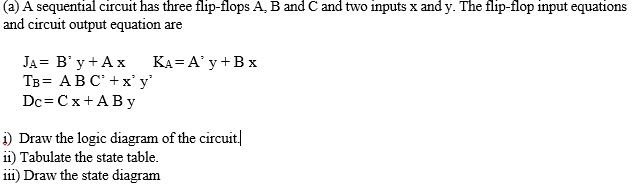
logic circuit question
Homework Answers
Request Answer!
We need at least 10 more requests to produce the answer.
0 / 10 have requested this problem solution
The more requests, the faster the answer.
The following information relates to GC Company for the current year:
 Capture.JPG
Tricycle Ltd produces three joint products, A, B and C. These products become identifiable after the first process but are processed further before being sold.
Capture.JPG
The management of Vulture Ltd decided to prepare a cash budget for April and May. The following information is available:
Capture.JPG
Optoelectronics
Capture.JPG
answer for P1.6
Capture-2.JPGCapture-1.JPGCapture.JPG
Problem 6-4A Preparing a bank reconciliation and recording adjustments LO P3
Capture 2.JPGCapture 3.JPGCapture.JPGpart 1 and 2 - for part 2 all journal entries needed
statistics
 <p><img src="https://img.homeworklib.com/uploads/ueditor/20210712/1626136930105630.jpg" title="1626136930105630.jpg" alt="Capture.JPG"/></p>
subject: (digital circuit: Sequential LOGIC CIRCUIT.) Question: 1. Write the program code in VHDL to create...
subject: (digital circuit: Sequential LOGIC CIRCUIT.) Question: 1. Write the program code in VHDL to create a simple OR application with 3 input , complete with its library, entity and architecture! 2. Explain the working principle of PAL and GAL! Search the IC GAL22V10D datasheet! and also Draw and explain the function of the legs of IC GAL22V10D!
Question 14 Question 15 Draw the logic circuit and write the HDL implementation for a FullAdder u...
 Question 14 Question 15 Draw the logic circuit and write the HDL implementation for a FullAdder using HalfAdder and Or chips. Clearly label the chips and internal wires with the names used in your HDL. Draw the logic circuit and write HDL code for a RAM with 2 registers using Register, Mux16, and Dmux chips. Clearly label the chips and intemal wires with the names used in your HDL HDL Chip FulLAdder HDL Chip RAM // The available chips: The...
For this problem, you are to design a simple combinational logic circuit The circuit is a...
For this problem, you are to design a simple combinational logic circuit The circuit is a 2- bit priority encoder with inputs I2 and I1 and outputs Z1 and Z0. The circuit behaves as follows: • If I2I1 = 00, then Z1Z0 = 00 (no active input) • If I2I1 = 01, then Z1Z0 = 01 (low-priority input, X1, is active) • If I2I1 = 1-, then Z1Z0 = 10 (high-priority input, X2, is active) Note that...
 Question 14 Question 15 Draw the logic circuit and write the HDL implementation for a FullAdder using HalfAdder and Or chips. Clearly label the chips and internal wires with the names used in your HDL. Draw the logic circuit and write HDL code for a RAM with 2 registers using Register, Mux16, and Dmux chips. Clearly label the chips and intemal wires with the names used in your HDL HDL Chip FulLAdder HDL Chip RAM // The available chips: The...
Most questions answered within 3 hours.
-
Where is the error in this code sequence?
String s1 = "Hello";
String s2 = "ello";...
asked 11 months ago -
Financial data for Joel de Paris, Inc., for last year
follow:
Joel de Paris, Inc.
Balance...
asked 11 months ago -
Consider this reaction:
Al2(SO4)3 (aq)+ BaCl3
(aq) Al2Cl6 (aq)- +
3BaSO4(s) . What is the...
asked 11 months ago -
Suppose that Savneet is considering increasing her
recent random sample from 20 car rentals to 40...
asked 11 months ago -
Trucks arrive at an unloading terminal at an average rate of 120
per hour.
Trucks arrive...
asked 11 months ago -
Why are methanol and ethanol completely soluble in water while
octanol is not very little soluble....
asked 11 months ago -
A facilities manager at a university reads in a research report
that the mean amount of...
asked 11 months ago -
When the CuSO4 is rehydrated by adding water to the anhydrous
compound, is this an endothermic...
asked 11 months ago -
A ray of sunlight is passing from diamond into crown glass; the
angle of incidence is...
asked 11 months ago -
A block of mass 0.249 kg is placed on top of a light, vertical
spring of...
asked 11 months ago -
how do the kidneys compensate in the presences of acidosis
a) trigger hyperventilate
b) reserve acid...
asked 11 months ago -
Question 501 pts
The rental rate of capital to the firm increases. Which of the
following...
asked 11 months ago