
Homework Answers
Add Answer to:
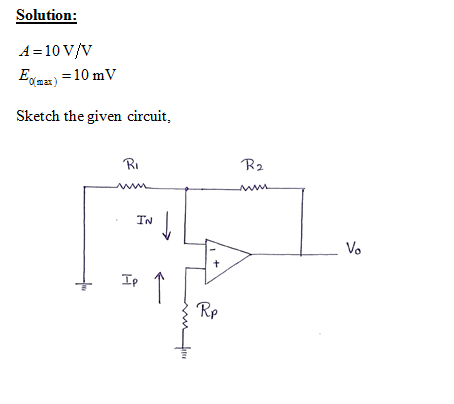
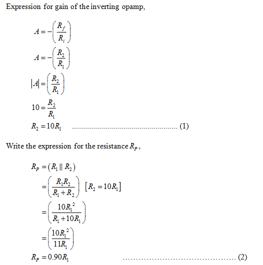
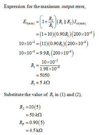
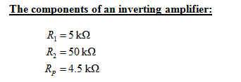
The circuit of Fig. 5.Sa is to be used as an inverting amplifier with a gain...
The gain of the non-inverting amplifier is set by the values of the resistors connected to the op...
 The gain of the non-inverting amplifier is set by the values of the resistors connected to the op- .amp can never be less than 1, even when RB is very high and RT equals 0 A voltage divider is a circuit involving two resistors in series All above is .1 correct Which statement not correct for Ideal operational amplifier Infinite open loop gain AOL for differential .1 .signa Zero gain for the common mode signal .Zero output impedance .noninfinite bandwidth...
2. Design a non-inverting op-amp circuit with two resistors under the following conditions: a. The gain of the ampl...
 2. Design a non-inverting op-amp circuit with two resistors under the following conditions: a. The gain of the amplifier must be +10 b. The input range is ± 2V c. The total power consumed by the resistors must be less than 100 mW Show all the calculations required to design the amplifier circuit with the shown specifications.in details Use MULTISIM to create the op-amp circuit and print a fully labelled diagram of the circuits with the voltmeters displays showing both...
2. Consider this non-inverting op-amp amplifier This non-inverting amplifier circuit uses an operational amplifier as a...
 2. Consider this non-inverting op-amp amplifier This non-inverting amplifier circuit uses an operational amplifier as a building block. Do around. The op-amp's gain is a "little a"), but the overall amplifier's gain is A Cbig A. Derive the value of the output voltage, ve, as a function of the input voltage not confuse the non-inverting amplifier with the operational amplifier that it is built a. and the op-amp's gain a. What is the overall amplifier's gain Avo/v? (20pts) b. We...
Inverting Amplifier Figure 4.2 shows the fundamental configuration of Op-Amp in which it is used as...
 Inverting Amplifier Figure 4.2 shows the fundamental configuration of Op-Amp in which it is used as an inverting amplifier. In this configuration the ratio, R2/R1 completely controls the effective gain of the amplifier and it can be verified that the output voltage is equal to Vo = - (R2/R1)Vin R2 100K Q-10V R1 Vinow 20K 1 2 7 V Vo 3 -10v Figure 4.2 Part 1 - Inverting Amp: Procedure 1. Construct the circuit of figure 4.2 using Op-Amp IC...
c) In estimating DC imperfections (input offset voltage, input offset current and the inverting amplifier with...
 c) In estimating DC imperfections (input offset voltage, input offset current and the inverting amplifier with nominal gain of -100 using 1 current) of an op-map, an and 10MQ resistors is implemented using the op-amp as shown in Fig 2(a) below R2 10MQ R 100k Vi Vo Figure 2(a): Inverting amplifier Measurements are conducted on the output voltage of the inverting amplifier under the following conditions: (i) the input (V) is open circuited and the output voltage is found to...
2.103 An inverting amplifier with nominal gain of-50 VIV employs an op amp having a dc...
 2.103 An inverting amplifier with nominal gain of-50 VIV employs an op amp having a dc gain of 10 and a unity-gain frequency of 10 Hz. What is the 3-dB frequency fd of the closed-loop amplifier? What is its gain at 0.1 fsd andat 10fsdB?
Sketch the circuit diagram for an inverting amplifier, and give component values that will produce a...
Sketch the circuit diagram for an inverting amplifier, and give component values that will produce a gain of 500. The op-amp has a supply voltage of ± 15 V. What is the input signal range that will avoid saturation? Show how the inverting amplifier circuit can be modified to provide gain to only the difference in voltage between two inputs signals, and give component values to make this differential gain equal to 500. If the common-mode rejection ratio (CMRR) for...
Sketch the circuit diagram for an inverting amplifier, and give component values that will produce a...
Sketch the circuit diagram for an inverting amplifier, and give component values that will produce a gain of 500. The op-amp has a supply voltage of ± 15 V. What is the input signal range that will avoid saturation? Show how the inverting amplifier circuit can be modified to provide gain to only the difference in voltage between two inputs signals, and give component values to make this differential gain equal to 500. If the common-mode rejection ratio (CMRR) for...
An op-amp is to be selected for an inverting amplifier to be used at dc and...
 An op-amp is to be selected for an inverting amplifier to be
used at dc and very low frequencies. A closed-loop nominal gain 0f
-100 is desired. Specifications indicate the minimum value of dc
open-loop gain cannot exceed 0.1dB. Assume in the design of problem
with the following additional specifications given:
dc output due to input offset voltage
100mV
dc output due to input offset voltage
5mV
Determine the maximum value of input offset voltage allowed for
the op-amp. If...
An op-amp is to be selected for an inverting amplifier to be
used at dc and very low frequencies. A closed-loop nominal gain 0f
-100 is desired. Specifications indicate the minimum value of dc
open-loop gain cannot exceed 0.1dB. Assume in the design of problem
with the following additional specifications given:
dc output due to input offset voltage
100mV
dc output due to input offset voltage
5mV
Determine the maximum value of input offset voltage allowed for
the op-amp. If...
Problem 1) [15 marks] The gain of the dual-op-axap instrumentation amplifier shown in Fig. 1 can be adjusted by the variable resistor Ro. The op-amps are ideal. atu Fig. 1 a)Show that v.-2(1 RG )...
 Problem 1) [15 marks] The gain of the dual-op-axap instrumentation amplifier shown in Fig. 1 can be adjusted by the variable resistor Ro. The op-amps are ideal. atu Fig. 1 a)Show that v.-2(1 RG )(v2-v.). b Specify suitable components to have a variable gain from 10 to 100 V/V. Problem 2) [15 marks] a) Design an op-amp limiter circuit for amplitude control with the transfer characteristic of Fig. 2(a). Use +-15V DC sources to power the circuit. Assume Vo-0.7 V...
 The gain of the non-inverting amplifier is set by the values of the resistors connected to the op- .amp can never be less than 1, even when RB is very high and RT equals 0 A voltage divider is a circuit involving two resistors in series All above is .1 correct Which statement not correct for Ideal operational amplifier Infinite open loop gain AOL for differential .1 .signa Zero gain for the common mode signal .Zero output impedance .noninfinite bandwidth...
 2. Design a non-inverting op-amp circuit with two resistors under the following conditions: a. The gain of the amplifier must be +10 b. The input range is ± 2V c. The total power consumed by the resistors must be less than 100 mW Show all the calculations required to design the amplifier circuit with the shown specifications.in details Use MULTISIM to create the op-amp circuit and print a fully labelled diagram of the circuits with the voltmeters displays showing both...
 2. Consider this non-inverting op-amp amplifier This non-inverting amplifier circuit uses an operational amplifier as a building block. Do around. The op-amp's gain is a "little a"), but the overall amplifier's gain is A Cbig A. Derive the value of the output voltage, ve, as a function of the input voltage not confuse the non-inverting amplifier with the operational amplifier that it is built a. and the op-amp's gain a. What is the overall amplifier's gain Avo/v? (20pts) b. We...
 Inverting Amplifier Figure 4.2 shows the fundamental configuration of Op-Amp in which it is used as an inverting amplifier. In this configuration the ratio, R2/R1 completely controls the effective gain of the amplifier and it can be verified that the output voltage is equal to Vo = - (R2/R1)Vin R2 100K Q-10V R1 Vinow 20K 1 2 7 V Vo 3 -10v Figure 4.2 Part 1 - Inverting Amp: Procedure 1. Construct the circuit of figure 4.2 using Op-Amp IC...
 c) In estimating DC imperfections (input offset voltage, input offset current and the inverting amplifier with nominal gain of -100 using 1 current) of an op-map, an and 10MQ resistors is implemented using the op-amp as shown in Fig 2(a) below R2 10MQ R 100k Vi Vo Figure 2(a): Inverting amplifier Measurements are conducted on the output voltage of the inverting amplifier under the following conditions: (i) the input (V) is open circuited and the output voltage is found to...
 2.103 An inverting amplifier with nominal gain of-50 VIV employs an op amp having a dc gain of 10 and a unity-gain frequency of 10 Hz. What is the 3-dB frequency fd of the closed-loop amplifier? What is its gain at 0.1 fsd andat 10fsdB?
 An op-amp is to be selected for an inverting amplifier to be
used at dc and very low frequencies. A closed-loop nominal gain 0f
-100 is desired. Specifications indicate the minimum value of dc
open-loop gain cannot exceed 0.1dB. Assume in the design of problem
with the following additional specifications given:
dc output due to input offset voltage
100mV
dc output due to input offset voltage
5mV
Determine the maximum value of input offset voltage allowed for
the op-amp. If...
An op-amp is to be selected for an inverting amplifier to be
used at dc and very low frequencies. A closed-loop nominal gain 0f
-100 is desired. Specifications indicate the minimum value of dc
open-loop gain cannot exceed 0.1dB. Assume in the design of problem
with the following additional specifications given:
dc output due to input offset voltage
100mV
dc output due to input offset voltage
5mV
Determine the maximum value of input offset voltage allowed for
the op-amp. If...
 Problem 1) [15 marks] The gain of the dual-op-axap instrumentation amplifier shown in Fig. 1 can be adjusted by the variable resistor Ro. The op-amps are ideal. atu Fig. 1 a)Show that v.-2(1 RG )(v2-v.). b Specify suitable components to have a variable gain from 10 to 100 V/V. Problem 2) [15 marks] a) Design an op-amp limiter circuit for amplitude control with the transfer characteristic of Fig. 2(a). Use +-15V DC sources to power the circuit. Assume Vo-0.7 V...
Most questions answered within 3 hours.
-
Where is the error in this code sequence?
String s1 = "Hello";
String s2 = "ello";...
asked 11 months ago -
Financial data for Joel de Paris, Inc., for last year
follow:
Joel de Paris, Inc.
Balance...
asked 11 months ago -
Consider this reaction:
Al2(SO4)3 (aq)+ BaCl3
(aq) Al2Cl6 (aq)- +
3BaSO4(s) . What is the...
asked 11 months ago -
Suppose that Savneet is considering increasing her
recent random sample from 20 car rentals to 40...
asked 11 months ago -
Trucks arrive at an unloading terminal at an average rate of 120
per hour.
Trucks arrive...
asked 11 months ago -
Why are methanol and ethanol completely soluble in water while
octanol is not very little soluble....
asked 11 months ago -
A facilities manager at a university reads in a research report
that the mean amount of...
asked 11 months ago -
When the CuSO4 is rehydrated by adding water to the anhydrous
compound, is this an endothermic...
asked 11 months ago -
A ray of sunlight is passing from diamond into crown glass; the
angle of incidence is...
asked 11 months ago -
A block of mass 0.249 kg is placed on top of a light, vertical
spring of...
asked 11 months ago -
how do the kidneys compensate in the presences of acidosis
a) trigger hyperventilate
b) reserve acid...
asked 11 months ago -
Question 501 pts
The rental rate of capital to the firm increases. Which of the
following...
asked 11 months ago