

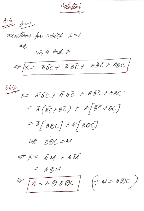
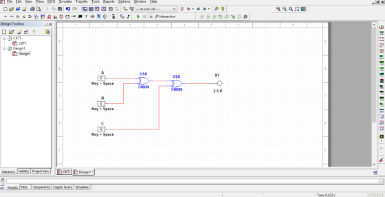
![3.6 Question [2 marks] 3.6.1 Write a Boolean expression in SOP format for the following Truth Table. [0.5 mark] 3.6.2 Use Boo](http://img.homeworklib.com/questions/acec8ba0-62f3-11eb-886f-0f4a6c9ed4f1.png?x-oss-process=image/resize,w_560)
Homework Answers
Solution:
3.4.1 AND 3.4.2
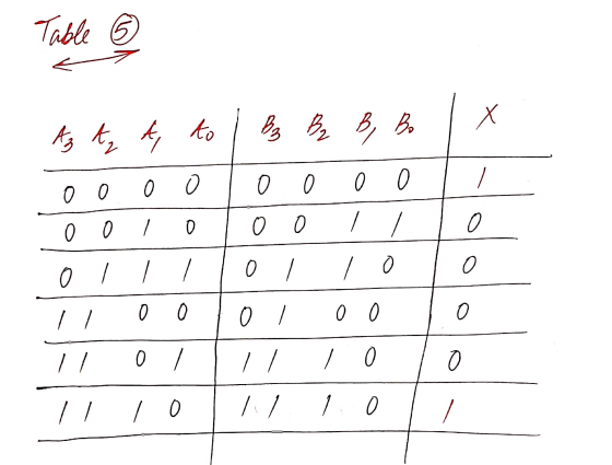
AS CAN BE CONCLUDED FROM TABLE 5....FOR FIRST AND THE LAST COMBINATION THE INPUTS ARE SAME AND THE LED GLOWS
BINARY INPUTS IN THE ORDER A3 A2 A1 A0 B3 B2 B1 B0
0000 0000

0010 0011
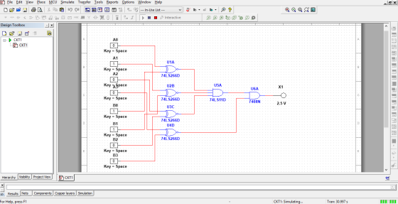
0111 0110
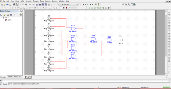
1100 0100
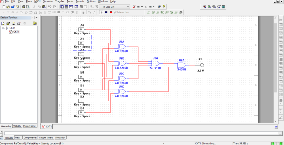
1101 1110
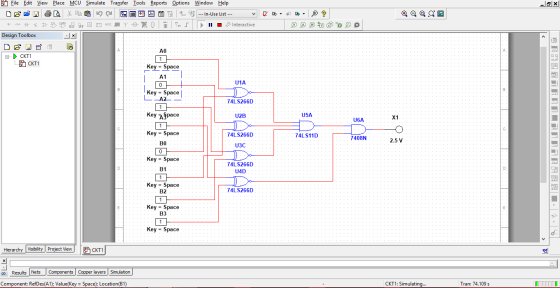
1110 1110

TABLE 5
---------------------------------------------------------------------------------------------------------------------------
PART 3.5.1 AND 3.5.2
OUTPUTS
X3 X2 X1 X0 FOR
D1 = 0 AND
A3 A2 A1 A0 = 0000
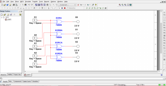
A3 A2 A1 A0 = 0010

A3 A2 A1 A0 = 0111
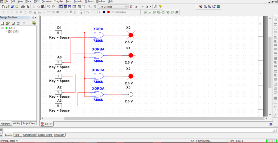
A3 A2 A1 A0 = 1100
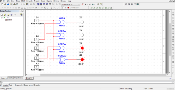
A3 A2 A1 A0 = 1101
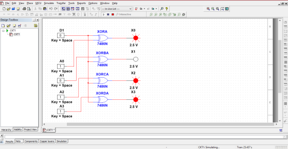
A3 A2 A1 A0 = 1110
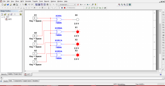
OUTPUTS
X3 X2 X1 X0 FOR
D1 = 1 AND
A3 A2 A1 A0 = 0000
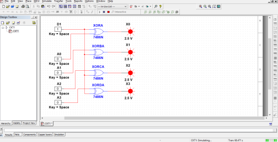
A3 A2 A1 A0 = 0010

A3 A2 A1 A0 = 0111

A3 A2 A1 A0 = 1100

A3 A2 A1 A0 = 1101

A3 A2 A1 A0 = 1110
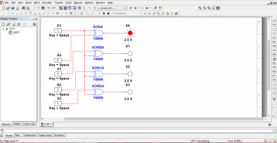
------------------------------------------------------------------------------------------------------------------------
PART 3.6
Add Answer to:
3.4.1 Build and simulate the comparator circuit shown in Figure 3, in Multisim. The inputs A3,...
3. PRELAB 1. A half adder is a circuit that has two inputs, A and B,...
 3. PRELAB 1. A half adder is a circuit that has two inputs, A and B, and two outputs, sum and carry. It adds A and B according to the rules of binary addition and outputs the sum and carry. Design a half-adder circuit using one XOR gate and one AND gate. Verify your design through truth table and with Multisim. 2. Whereas the half adder added two inputs A and B, the full adder adds three inputs together, A,...
Create a combinatorial circuit that performs a 3 bit multiplication. The circuit will have two 3-bit...
Create a combinatorial circuit that performs a 3 bit multiplication. The circuit will have two 3-bit inputs A2 A1 A0 and B2 B1 B0 and one 6 bit output. Create a combinatorial circuit that performs a 3-bit multiplication. The circuit will accept two 3-bit inputs A2 A1 A0 and B2 B1 B0 and generate one 6 bit output. First, create 3 Integrated circuits (iC). The first IC takes as input, B0, A2, A1, and A0 as input, and it generates...
A Y = A ® B 1 1 1 1 1 Apply the idea of the truth table above and design a 3-bit comparator using XOR or XNOR gates of...
 A Y = A ® B 1 1 1 1 1 Apply the idea of the truth table above and design a 3-bit comparator using XOR or XNOR gates of your choice. The design should be able to determine the equality between two 3-bit words. An LED should be turned ON only when every bit in "Word A" matches every corresponding bit in "Word B". Otherwise, the LED has to be OFF Hint for I/O port Definitions: Port Name Direction...
In Multisim, rewire your opamp circuit so that it matches the circuit in Figure 2 U1-....
 In Multisim, rewire your opamp circuit so that it matches the circuit in Figure 2 U1-. V4 1kn 0.707 Vrms z OPAMP 3T BASIC R1 0o Figure 2 10. Perform a transient analysis on the circuit. Plot both the input signal (node 3 in Figure 1), and the output (node 1 in Figure 1) on the same graph. Set the time start and end time of the plot to start at zero and run for approximately two cycles of the...
Truth Table Wire up the following 2-bit adder circuit shown in Figure 2. Connect the inputs...
 Truth Table
Wire up the following 2-bit adder circuit shown in Figure 2. Connect the inputs to the logic switches on the proto-burnd and the outputs to the LED indicators. Fill out a truth table for all 16 combinations of the input switches, and verify that the circuit behaves as expected Disconnect the Ao bit from the switch and connect it to the TTL function generator. Set bit A1 to 0 and Bo and B to . Measure the propagation...
Truth Table
Wire up the following 2-bit adder circuit shown in Figure 2. Connect the inputs to the logic switches on the proto-burnd and the outputs to the LED indicators. Fill out a truth table for all 16 combinations of the input switches, and verify that the circuit behaves as expected Disconnect the Ao bit from the switch and connect it to the TTL function generator. Set bit A1 to 0 and Bo and B to . Measure the propagation...
Help me please. How can I do this question. Consider the circuit shown in (Figure 1)....
 Help me please. How can I do this question.
Consider the circuit shown in (Figure 1). Suppose that ig equals 9e-5 A. Part A Use the Fourier transform to find i, (t). Suppose that io (t) = Aje-atu(t) + A2e-02* u(t) + Azeztul-t), where az > 21. Determine the va of Aj, aj, A2, a2, A3, and az. Express your answers using three significant figures separated by commas. Express A2, and A3 in amperes. Express 21, 22, and as in...
Help me please. How can I do this question.
Consider the circuit shown in (Figure 1). Suppose that ig equals 9e-5 A. Part A Use the Fourier transform to find i, (t). Suppose that io (t) = Aje-atu(t) + A2e-02* u(t) + Azeztul-t), where az > 21. Determine the va of Aj, aj, A2, a2, A3, and az. Express your answers using three significant figures separated by commas. Express A2, and A3 in amperes. Express 21, 22, and as in...
EE252 100 Points Digital Design I Two's Complement Subtraction and Add / Subtract Circuits Homework 3....
 EE252 100 Points Digital Design I Two's Complement Subtraction and Add / Subtract Circuits Homework 3. (25 Pts) The following circuit uses two 7483 (4-bit adder) ICs, labeled 7483-1 and 7483-2, respectively. Answer the questions for EACH of the following THREE CASES: Case 1: D=0010, and E = 0110 Case 2: D = 1000, and E = 0101 Case 3: D = 1000, and E = 1001 a. (6 Pts - 2 Pts per Case) What are the binary inputs...
I need help completing this in multisim 8. Load the circuit E6B-3.MS7, shown in Figure 6B.3....
 I need help completing this in multisim
8. Load the circuit E6B-3.MS7, shown in Figure 6B.3. Page 2 of 4 Module 3: Laboratory 2B: Shift Registers .5V 41958 Figure 6B.3: Pseudorandom pattem generator 9. Simulate the circuit. Record the output patterns in Table 6B.1. Pattern ABCD Pattern ABCD 10 12 13 14 15 Table 6B.1: Pattem generator output patterns 0. Experiment with different feedback imputs for the XNOR gate. What do you find?
I need help completing this in multisim
8. Load the circuit E6B-3.MS7, shown in Figure 6B.3. Page 2 of 4 Module 3: Laboratory 2B: Shift Registers .5V 41958 Figure 6B.3: Pseudorandom pattem generator 9. Simulate the circuit. Record the output patterns in Table 6B.1. Pattern ABCD Pattern ABCD 10 12 13 14 15 Table 6B.1: Pattem generator output patterns 0. Experiment with different feedback imputs for the XNOR gate. What do you find?
Q5) A combinational circuit with internal signals and signal propagation delays Shown below is a combination...
 Q5) A combinational circuit with internal signals and signal propagation delays Shown below is a combination circuit that takes 5 inputs (LO L1, L2, L3, and Comp), and generates 4 outputs (L4, L5, L6, し7) Please design the entity as well as the test bench for this combinational circuit. In your design, please set up internal signals Al, B, A2, B2, A3, B3, A4, B4, A5, B5, A6, B6, A7 and B7 Your entity design is Your test bench design...
microprocessors,,pls help.. 1. (3 Points) Draw a timing diagram similar to the 'practical' case of figure...
 microprocessors,,pls help..
1. (3 Points) Draw a timing diagram similar to the 'practical' case of figure 5, below, for the case where signal Ao makes its transition first. Note: For each timing diagram that you draw, be sure that subsequent events appear to the right of causative events, and show causality arrows. 3.1 Glitch pulses Consider the one-bit adder circuit of figure 4. This circuit is called a one-bit (binary) adder because output signal So is the sum of input...
microprocessors,,pls help..
1. (3 Points) Draw a timing diagram similar to the 'practical' case of figure 5, below, for the case where signal Ao makes its transition first. Note: For each timing diagram that you draw, be sure that subsequent events appear to the right of causative events, and show causality arrows. 3.1 Glitch pulses Consider the one-bit adder circuit of figure 4. This circuit is called a one-bit (binary) adder because output signal So is the sum of input...
 3. PRELAB 1. A half adder is a circuit that has two inputs, A and B, and two outputs, sum and carry. It adds A and B according to the rules of binary addition and outputs the sum and carry. Design a half-adder circuit using one XOR gate and one AND gate. Verify your design through truth table and with Multisim. 2. Whereas the half adder added two inputs A and B, the full adder adds three inputs together, A,...
 A Y = A ® B 1 1 1 1 1 Apply the idea of the truth table above and design a 3-bit comparator using XOR or XNOR gates of your choice. The design should be able to determine the equality between two 3-bit words. An LED should be turned ON only when every bit in "Word A" matches every corresponding bit in "Word B". Otherwise, the LED has to be OFF Hint for I/O port Definitions: Port Name Direction...
 In Multisim, rewire your opamp circuit so that it matches the circuit in Figure 2 U1-. V4 1kn 0.707 Vrms z OPAMP 3T BASIC R1 0o Figure 2 10. Perform a transient analysis on the circuit. Plot both the input signal (node 3 in Figure 1), and the output (node 1 in Figure 1) on the same graph. Set the time start and end time of the plot to start at zero and run for approximately two cycles of the...
 Truth Table
Wire up the following 2-bit adder circuit shown in Figure 2. Connect the inputs to the logic switches on the proto-burnd and the outputs to the LED indicators. Fill out a truth table for all 16 combinations of the input switches, and verify that the circuit behaves as expected Disconnect the Ao bit from the switch and connect it to the TTL function generator. Set bit A1 to 0 and Bo and B to . Measure the propagation...
Truth Table
Wire up the following 2-bit adder circuit shown in Figure 2. Connect the inputs to the logic switches on the proto-burnd and the outputs to the LED indicators. Fill out a truth table for all 16 combinations of the input switches, and verify that the circuit behaves as expected Disconnect the Ao bit from the switch and connect it to the TTL function generator. Set bit A1 to 0 and Bo and B to . Measure the propagation...
 Help me please. How can I do this question.
Consider the circuit shown in (Figure 1). Suppose that ig equals 9e-5 A. Part A Use the Fourier transform to find i, (t). Suppose that io (t) = Aje-atu(t) + A2e-02* u(t) + Azeztul-t), where az > 21. Determine the va of Aj, aj, A2, a2, A3, and az. Express your answers using three significant figures separated by commas. Express A2, and A3 in amperes. Express 21, 22, and as in...
Help me please. How can I do this question.
Consider the circuit shown in (Figure 1). Suppose that ig equals 9e-5 A. Part A Use the Fourier transform to find i, (t). Suppose that io (t) = Aje-atu(t) + A2e-02* u(t) + Azeztul-t), where az > 21. Determine the va of Aj, aj, A2, a2, A3, and az. Express your answers using three significant figures separated by commas. Express A2, and A3 in amperes. Express 21, 22, and as in...
 EE252 100 Points Digital Design I Two's Complement Subtraction and Add / Subtract Circuits Homework 3. (25 Pts) The following circuit uses two 7483 (4-bit adder) ICs, labeled 7483-1 and 7483-2, respectively. Answer the questions for EACH of the following THREE CASES: Case 1: D=0010, and E = 0110 Case 2: D = 1000, and E = 0101 Case 3: D = 1000, and E = 1001 a. (6 Pts - 2 Pts per Case) What are the binary inputs...
 I need help completing this in multisim
8. Load the circuit E6B-3.MS7, shown in Figure 6B.3. Page 2 of 4 Module 3: Laboratory 2B: Shift Registers .5V 41958 Figure 6B.3: Pseudorandom pattem generator 9. Simulate the circuit. Record the output patterns in Table 6B.1. Pattern ABCD Pattern ABCD 10 12 13 14 15 Table 6B.1: Pattem generator output patterns 0. Experiment with different feedback imputs for the XNOR gate. What do you find?
I need help completing this in multisim
8. Load the circuit E6B-3.MS7, shown in Figure 6B.3. Page 2 of 4 Module 3: Laboratory 2B: Shift Registers .5V 41958 Figure 6B.3: Pseudorandom pattem generator 9. Simulate the circuit. Record the output patterns in Table 6B.1. Pattern ABCD Pattern ABCD 10 12 13 14 15 Table 6B.1: Pattem generator output patterns 0. Experiment with different feedback imputs for the XNOR gate. What do you find?
 Q5) A combinational circuit with internal signals and signal propagation delays Shown below is a combination circuit that takes 5 inputs (LO L1, L2, L3, and Comp), and generates 4 outputs (L4, L5, L6, し7) Please design the entity as well as the test bench for this combinational circuit. In your design, please set up internal signals Al, B, A2, B2, A3, B3, A4, B4, A5, B5, A6, B6, A7 and B7 Your entity design is Your test bench design...
 microprocessors,,pls help..
1. (3 Points) Draw a timing diagram similar to the 'practical' case of figure 5, below, for the case where signal Ao makes its transition first. Note: For each timing diagram that you draw, be sure that subsequent events appear to the right of causative events, and show causality arrows. 3.1 Glitch pulses Consider the one-bit adder circuit of figure 4. This circuit is called a one-bit (binary) adder because output signal So is the sum of input...
microprocessors,,pls help..
1. (3 Points) Draw a timing diagram similar to the 'practical' case of figure 5, below, for the case where signal Ao makes its transition first. Note: For each timing diagram that you draw, be sure that subsequent events appear to the right of causative events, and show causality arrows. 3.1 Glitch pulses Consider the one-bit adder circuit of figure 4. This circuit is called a one-bit (binary) adder because output signal So is the sum of input...
Most questions answered within 3 hours.
-
Where is the error in this code sequence?
String s1 = "Hello";
String s2 = "ello";...
asked 11 months ago -
Financial data for Joel de Paris, Inc., for last year
follow:
Joel de Paris, Inc.
Balance...
asked 11 months ago -
Consider this reaction:
Al2(SO4)3 (aq)+ BaCl3
(aq) Al2Cl6 (aq)- +
3BaSO4(s) . What is the...
asked 11 months ago -
Suppose that Savneet is considering increasing her
recent random sample from 20 car rentals to 40...
asked 11 months ago -
Trucks arrive at an unloading terminal at an average rate of 120
per hour.
Trucks arrive...
asked 11 months ago -
Why are methanol and ethanol completely soluble in water while
octanol is not very little soluble....
asked 11 months ago -
A facilities manager at a university reads in a research report
that the mean amount of...
asked 11 months ago -
When the CuSO4 is rehydrated by adding water to the anhydrous
compound, is this an endothermic...
asked 11 months ago -
A ray of sunlight is passing from diamond into crown glass; the
angle of incidence is...
asked 11 months ago -
A block of mass 0.249 kg is placed on top of a light, vertical
spring of...
asked 11 months ago -
how do the kidneys compensate in the presences of acidosis
a) trigger hyperventilate
b) reserve acid...
asked 11 months ago -
Question 501 pts
The rental rate of capital to the firm increases. Which of the
following...
asked 11 months ago