

Homework Answers

Add Answer to:
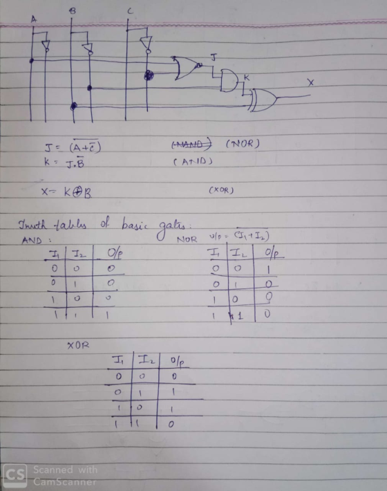
X 1. Determine the truth table for the above circuit. A B C 0 0 0...
3. For the following circuit: B a. Give the truth table for F. b. Complete the...
 3. For the following circuit: B a. Give the truth table for F. b. Complete the following K-map and use it to give the minimized POS form for F(A,B,C). CIAB 00 01 11 10 C. Use boolean axioms and theorems on POS expression obtained in (b) to get the SOP form. The final SOP expression should have a maximum of two terms. d. Draw the logic circuit for the SOP form.
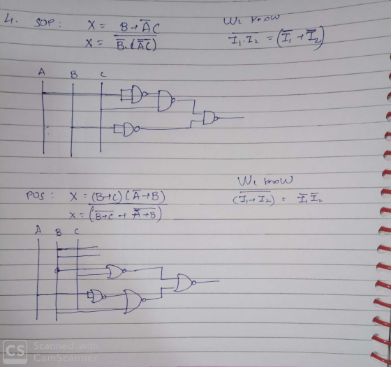
Create a truth table to implement AND logic using only NAND gates. Draw the circuit diagram...
Create a truth table to implement AND logic using only NAND gates. Draw the circuit diagram (schematic) for the implementation. Do the same for OR logic using only NOR gates.
(1)Try to use NAND gates to achieve the truth table function of an XOR gate (2)...
(1)Try to use NAND gates to achieve the truth table function of an XOR gate (2) Try to design a clicker for three people, it just needs two people to agree to pass. A,B,C indicate the people, 0 means don't agree, 1 means agree. If it passes the result is 1. Please write the truth table, the SOP (sum of products) equation and draw the logic circuit for it. (3)Use a Karnaugh-map to simplify the following Boolean function: F= AB'C'+A'B'C'+AB'C+A'B'C+AB...
Consider the following logic: F = ΣW,X,Y,Z (0x1, 0x5, 0x8, 0xA, 0xB, 0xC, 0xE, 0xF). And...
Consider the following logic: F = ΣW,X,Y,Z (0x1, 0x5, 0x8, 0xA, 0xB, 0xC, 0xE, 0xF). And 0x2, 0x4 and 0x6 are “don't care” cases. a) Draw a K-map and write a minimized SOP expression for this circuit. Include grouping circles for a minimized SOP expression. b) Draw the minimized SOP circuit using only NAND gates. c) Are there any static hazards? If so, write the Boolean expression to resolve any static hazards?
(18 pts) Given the Boolean function F(A, B, C, D) = Σ (0, 1, 2, 3,...
 (18 pts) Given the Boolean function F(A, B, C, D) = Σ (0, 1, 2, 3, 4, 5, 7, 8, 10, 12, 14) a. Draw a Karnaugh Map. b. Identify the prime implicants of F. c. Identify all Essential Prime Implicants of F. d. Derive minimal SOP expressions for F e. Derive minimal POS expressions for F. f. Assume each inverter has a cost of 1, each 2-input NAND gate has a cost of 2, and 4-input NAND gate has...
Build a digital circuit that can add two binary numbers of two bit each and shows...
 Build a digital circuit that can add two binary numbers of two
bit each and shows the answer using three LEDs
1. Find the canonical equations of the following characteristics
table in SOP and POS
2. Convert them and implement the SOP canonical equation
only.
3. Simplify each equation SOP and POS and implement each one
using logic gates.
4. Convert each circuit into its respective NAND-NAND and
NOR_NOR and implement them using logic gates.
Objetivo: Construir un circuito digital...
Build a digital circuit that can add two binary numbers of two
bit each and shows the answer using three LEDs
1. Find the canonical equations of the following characteristics
table in SOP and POS
2. Convert them and implement the SOP canonical equation
only.
3. Simplify each equation SOP and POS and implement each one
using logic gates.
4. Convert each circuit into its respective NAND-NAND and
NOR_NOR and implement them using logic gates.
Objetivo: Construir un circuito digital...
A combination circuit is specified by the following Boolean functions listed below. h(a, b, c) = b,c' + a'c Implement the circuit with a 3x8 decoder. Provide truth table and drawing the l...
 A combination circuit is specified by the following Boolean functions listed below. h(a, b, c) = b,c' + a'c Implement the circuit with a 3x8 decoder. Provide truth table and drawing the logic/circuit diagram. Use the block diagram for the decoder provided in Figure A4 in supplements. Please label the inputs and outputs clearly. Note: use single 3x8 decoder Question 2 (15 points] A priority encoder is an encoder circuit that includes the Truth Table of a priority function. The...
Question 2 1. Formulate the minimized SOP and POS Boolean expression for the following truth table...
 Question 2 1. Formulate the minimized SOP and POS Boolean expression for the following truth table using Karnaugh map techniques. Out of the SOP and POS implementations, which is cheaper in terms of number of transistors? You can assume two transistors per input for a gate. (10 points) A B C Output 0 0 0 1 1 0 0 1 0 1 0 0 0 1 0 1 1
Consider the following function. (8 <A ri eve n of products) expression. Don't draw the gate...
 Consider the following function. (8 <A ri eve n of products) expression. Don't draw the gate 1131 0 diagram yet. (b) Use De Morgan's Laws or "bubble pushing" to convert the SOP expression to something that can be directly implemented with only NAND/NOR/inverter gates. (c) Now draw the schematic (logic gates) for the resulting NAND/NOR/inverter circuit.
I need help with this Logic circuit problem. Problem #2 Given the logic function F(a,b,c) cabctab'c'+a'c'c'tabb'...
 I need help with this Logic circuit problem.
Problem #2 Given the logic function F(a,b,c) cabctab'c'+a'c'c'tabb' a) Normalize the product terms and write the function again. Answer: F(a,b,c) b) Find a minimal SOP expression using a Karnaugh Map Answer: F(a,b,c) c) Based on the result of the previous part find an expression that minimizes the discrete gate count using gates of any kinod. Answer: Fla,b,c)- d) Find a minimal POS expression using a Karnaugh Map Answer: F(a,b,c)
I need help with this Logic circuit problem.
Problem #2 Given the logic function F(a,b,c) cabctab'c'+a'c'c'tabb' a) Normalize the product terms and write the function again. Answer: F(a,b,c) b) Find a minimal SOP expression using a Karnaugh Map Answer: F(a,b,c) c) Based on the result of the previous part find an expression that minimizes the discrete gate count using gates of any kinod. Answer: Fla,b,c)- d) Find a minimal POS expression using a Karnaugh Map Answer: F(a,b,c)
 3. For the following circuit: B a. Give the truth table for F. b. Complete the following K-map and use it to give the minimized POS form for F(A,B,C). CIAB 00 01 11 10 C. Use boolean axioms and theorems on POS expression obtained in (b) to get the SOP form. The final SOP expression should have a maximum of two terms. d. Draw the logic circuit for the SOP form.
 (18 pts) Given the Boolean function F(A, B, C, D) = Σ (0, 1, 2, 3, 4, 5, 7, 8, 10, 12, 14) a. Draw a Karnaugh Map. b. Identify the prime implicants of F. c. Identify all Essential Prime Implicants of F. d. Derive minimal SOP expressions for F e. Derive minimal POS expressions for F. f. Assume each inverter has a cost of 1, each 2-input NAND gate has a cost of 2, and 4-input NAND gate has...
 Build a digital circuit that can add two binary numbers of two
bit each and shows the answer using three LEDs
1. Find the canonical equations of the following characteristics
table in SOP and POS
2. Convert them and implement the SOP canonical equation
only.
3. Simplify each equation SOP and POS and implement each one
using logic gates.
4. Convert each circuit into its respective NAND-NAND and
NOR_NOR and implement them using logic gates.
Objetivo: Construir un circuito digital...
Build a digital circuit that can add two binary numbers of two
bit each and shows the answer using three LEDs
1. Find the canonical equations of the following characteristics
table in SOP and POS
2. Convert them and implement the SOP canonical equation
only.
3. Simplify each equation SOP and POS and implement each one
using logic gates.
4. Convert each circuit into its respective NAND-NAND and
NOR_NOR and implement them using logic gates.
Objetivo: Construir un circuito digital...
 A combination circuit is specified by the following Boolean functions listed below. h(a, b, c) = b,c' + a'c Implement the circuit with a 3x8 decoder. Provide truth table and drawing the logic/circuit diagram. Use the block diagram for the decoder provided in Figure A4 in supplements. Please label the inputs and outputs clearly. Note: use single 3x8 decoder Question 2 (15 points] A priority encoder is an encoder circuit that includes the Truth Table of a priority function. The...
 Question 2 1. Formulate the minimized SOP and POS Boolean expression for the following truth table using Karnaugh map techniques. Out of the SOP and POS implementations, which is cheaper in terms of number of transistors? You can assume two transistors per input for a gate. (10 points) A B C Output 0 0 0 1 1 0 0 1 0 1 0 0 0 1 0 1 1
 Consider the following function. (8 <A ri eve n of products) expression. Don't draw the gate 1131 0 diagram yet. (b) Use De Morgan's Laws or "bubble pushing" to convert the SOP expression to something that can be directly implemented with only NAND/NOR/inverter gates. (c) Now draw the schematic (logic gates) for the resulting NAND/NOR/inverter circuit.
 I need help with this Logic circuit problem.
Problem #2 Given the logic function F(a,b,c) cabctab'c'+a'c'c'tabb' a) Normalize the product terms and write the function again. Answer: F(a,b,c) b) Find a minimal SOP expression using a Karnaugh Map Answer: F(a,b,c) c) Based on the result of the previous part find an expression that minimizes the discrete gate count using gates of any kinod. Answer: Fla,b,c)- d) Find a minimal POS expression using a Karnaugh Map Answer: F(a,b,c)
I need help with this Logic circuit problem.
Problem #2 Given the logic function F(a,b,c) cabctab'c'+a'c'c'tabb' a) Normalize the product terms and write the function again. Answer: F(a,b,c) b) Find a minimal SOP expression using a Karnaugh Map Answer: F(a,b,c) c) Based on the result of the previous part find an expression that minimizes the discrete gate count using gates of any kinod. Answer: Fla,b,c)- d) Find a minimal POS expression using a Karnaugh Map Answer: F(a,b,c)
Most questions answered within 3 hours.
-
Where is the error in this code sequence?
String s1 = "Hello";
String s2 = "ello";...
asked 11 months ago -
Financial data for Joel de Paris, Inc., for last year
follow:
Joel de Paris, Inc.
Balance...
asked 11 months ago -
Consider this reaction:
Al2(SO4)3 (aq)+ BaCl3
(aq) Al2Cl6 (aq)- +
3BaSO4(s) . What is the...
asked 11 months ago -
Suppose that Savneet is considering increasing her
recent random sample from 20 car rentals to 40...
asked 11 months ago -
Trucks arrive at an unloading terminal at an average rate of 120
per hour.
Trucks arrive...
asked 11 months ago -
Why are methanol and ethanol completely soluble in water while
octanol is not very little soluble....
asked 11 months ago -
A facilities manager at a university reads in a research report
that the mean amount of...
asked 11 months ago -
When the CuSO4 is rehydrated by adding water to the anhydrous
compound, is this an endothermic...
asked 11 months ago -
A ray of sunlight is passing from diamond into crown glass; the
angle of incidence is...
asked 11 months ago -
A block of mass 0.249 kg is placed on top of a light, vertical
spring of...
asked 11 months ago -
how do the kidneys compensate in the presences of acidosis
a) trigger hyperventilate
b) reserve acid...
asked 11 months ago -
Question 501 pts
The rental rate of capital to the firm increases. Which of the
following...
asked 11 months ago