
Homework Answers

Add Answer to:
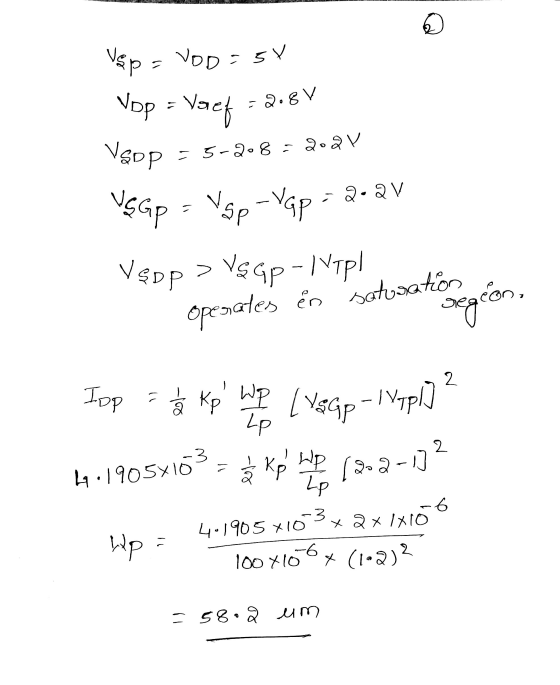
The following circuit creates a reference voltage, Vref. Assume VDD = 5 V Vref = 2.8...
The following circuit creates a reference voltage, Vref. Assume VDD = 5 V, Vref = 2.1...
 The following circuit creates a reference voltage, Vref. Assume VDD = 5 V, Vref = 2.1 V, Wn = 14 um, Lp=Ln = 1 um. Transistor parameters; kn' = 100 PAN2, kp' = 40 JANV2, VTon = 1 V, VTOp = -1 V. Calculate Wp in um. VDD Mp (Wp/Lp) Vref (Wn/Ln) Mn
Problem 1. The following circuit is used to create a voltage reference, Vref. Transistor Parameters are;...
 Problem 1. The following circuit is used to create a voltage reference, Vref. Transistor Parameters are; kn - 100 A/V2 and VT-1 V. Derive a symbolic expression for Vref. + VDD Vref (W/L) Figure 1 Voltage reference circuit
help with problem Problem 1. The following circuit is used to create a voltage reference, Vref....
 help with problem
Problem 1. The following circuit is used to create a voltage reference, Vref. Transistor Parameters are; kn = 100 PA/V and VT = 1 V. Derive a symbolic expression for Vref. + VDD R} + Vref (W/L) Figure 1 Voltage reference circuit
help with problem
Problem 1. The following circuit is used to create a voltage reference, Vref. Transistor Parameters are; kn = 100 PA/V and VT = 1 V. Derive a symbolic expression for Vref. + VDD R} + Vref (W/L) Figure 1 Voltage reference circuit
Consider a static CMOS inverter with the following parameters: VDD = 1.2V, Vtn = 0.48V, Vtp...
Consider a static CMOS inverter with the following parameters: VDD = 1.2V, Vtn = 0.48V, Vtp = -0.46V, kp' = μp*Cox = 40μA/V2, kn'= μnCox = 90μA/V2, Wn/Ln = 6, Wp/Lp = 12, Ec,nLn= 0.4V, Ec,pLp = 1.8V, Vsat,n = 124,340 m/s. Calculate the noise margins of the circuit using the Short-Channel Formula.
An analogue amplifier circuit is shown in Figure 1 below. VDD Q5 15V JL - Vout...
 An analogue amplifier circuit is shown in Figure 1 below. VDD Q5 15V JL - Vout Irer RI Vina JET T7T Figure 1 Integrated amplifier circuit. Circuit Data: Vpp = 15 V, IREF = I1 = I2 = 1.0 mA Transistor Data: Q1: NMOS, un Cox = 80 A/V?, W/L = 100 um/0.8 um, Vtn = 0.8 V, L = 0.10 um/V Q2: NPN BJT, B = 100, Vbe = 0.7 V, VA = 150 V Q3, Q4: NMOS, un...
5. The NMOS and PMOS transistors in the below circuit are matched with kn’(Wn/Ln)=kp'(Wp/Lp)=1 mA/V2 and...
 5. The NMOS and PMOS transistors in the below circuit are matched with kn’(Wn/Ln)=kp'(Wp/Lp)=1 mA/V2 and Vin=-Vt=1V. (20 pts) +5 V a) Which MOSFET is cut-off, NMOS (QN) or PMOS (QP) for VF-5V? Why (5 pts) Qp -5 Vo Ipp Vo VION ON -5 V b) When VF-5V, in which mode, saturation or triode, the circuit operate? Explain why? (5 pts) c) Find the drain current ipy and ipp and the voltage vo for VF-5V (10 pts)
Transistor parameters cm 1 Po=1V or Hm = 560 gdo cm rn = 0.6V Cio-1.7 m=...
 Transistor parameters cm 1 Po=1V or Hm = 560 gdo cm rn = 0.6V Cio-1.7 m= (bottom) 2 Ln = Lp = 0.25um ½,--0.6V Ciswoー0.4 (sidewall) m vad =2.SI. I0-10-A Q2. (40 pts). For an inverter. Wn-0.36 and WP-0.8μm. (a) Find the switching voltage VM (b) Calculate the values of Rn and Rp (c) We would now like to construct an inverter whose switching voltage is exactly half of the supply voltage. How would vou size the transistors? (d) The...
Given the circuit below with the following parameters: - M1: Vt,n = 0.48 V, Un Cox...
 Given the circuit below with the following parameters: - M1: Vt,n = 0.48 V, Un Cox = 90 UA/V2, W/L = 10 um/4 um, VdD+Vad 1 = 0.01 [1/V] - Supply voltage: Vpp = 3.3 V, vad = 10 mV > R a. Find the value of resistor R so that the bias current is 10uA. (Hint: Channel length modulation should be considered.) Ipi M1 Use the resistor value in (a) for the following calculations: b. What configuration (connection) M1...
Consider the following circuit. Assume the threshold voltage of the N-FETs is Vthn 0.4V, and threshold...
 Consider the following circuit. Assume the threshold voltage of the N-FETs is Vthn 0.4V, and threshold voltage of the PFET is Vthp-0.6V. Assume, both PFETs and NFETs have same oxide thickness (tox 2nm), and v length (L22nm). Assume, supply voltage (VDD)-2.5% and mobility of NFET and PFET are given by: 나 = 1000 cm 2/V-s and μ,-0.5Hn. Assume, width of the N-FET is same of both inverter, and equal to Wn110nm. Width of PFETs (Wp) are also same for both...
Find VL and VH for the inverter circuit below. Circle your final answer. 5) +2.5 V o VDD 1.81 Kn-100 HA/V2 To0.6 V VTo-0.85v Uo UI 2.22 2ф,-0.6 V Neglect short channel effects (Based on the symbol of...
 Find VL and VH for the inverter circuit below. Circle your final answer. 5) +2.5 V o VDD 1.81 Kn-100 HA/V2 To0.6 V VTo-0.85v Uo UI 2.22 2ф,-0.6 V Neglect short channel effects (Based on the symbol of the transistor, you should be able to find the VTO of ML and MS. Go to the MOSFET symbol lookup table. You should very clearly provide reasons for the state of the transistor (cutoff, triode, saturation) to get credit.
Find VL and...
Find VL and VH for the inverter circuit below. Circle your final answer. 5) +2.5 V o VDD 1.81 Kn-100 HA/V2 To0.6 V VTo-0.85v Uo UI 2.22 2ф,-0.6 V Neglect short channel effects (Based on the symbol of the transistor, you should be able to find the VTO of ML and MS. Go to the MOSFET symbol lookup table. You should very clearly provide reasons for the state of the transistor (cutoff, triode, saturation) to get credit.
Find VL and...
 The following circuit creates a reference voltage, Vref. Assume VDD = 5 V, Vref = 2.1 V, Wn = 14 um, Lp=Ln = 1 um. Transistor parameters; kn' = 100 PAN2, kp' = 40 JANV2, VTon = 1 V, VTOp = -1 V. Calculate Wp in um. VDD Mp (Wp/Lp) Vref (Wn/Ln) Mn
 Problem 1. The following circuit is used to create a voltage reference, Vref. Transistor Parameters are; kn - 100 A/V2 and VT-1 V. Derive a symbolic expression for Vref. + VDD Vref (W/L) Figure 1 Voltage reference circuit
 help with problem
Problem 1. The following circuit is used to create a voltage reference, Vref. Transistor Parameters are; kn = 100 PA/V and VT = 1 V. Derive a symbolic expression for Vref. + VDD R} + Vref (W/L) Figure 1 Voltage reference circuit
help with problem
Problem 1. The following circuit is used to create a voltage reference, Vref. Transistor Parameters are; kn = 100 PA/V and VT = 1 V. Derive a symbolic expression for Vref. + VDD R} + Vref (W/L) Figure 1 Voltage reference circuit
 An analogue amplifier circuit is shown in Figure 1 below. VDD Q5 15V JL - Vout Irer RI Vina JET T7T Figure 1 Integrated amplifier circuit. Circuit Data: Vpp = 15 V, IREF = I1 = I2 = 1.0 mA Transistor Data: Q1: NMOS, un Cox = 80 A/V?, W/L = 100 um/0.8 um, Vtn = 0.8 V, L = 0.10 um/V Q2: NPN BJT, B = 100, Vbe = 0.7 V, VA = 150 V Q3, Q4: NMOS, un...
 5. The NMOS and PMOS transistors in the below circuit are matched with kn’(Wn/Ln)=kp'(Wp/Lp)=1 mA/V2 and Vin=-Vt=1V. (20 pts) +5 V a) Which MOSFET is cut-off, NMOS (QN) or PMOS (QP) for VF-5V? Why (5 pts) Qp -5 Vo Ipp Vo VION ON -5 V b) When VF-5V, in which mode, saturation or triode, the circuit operate? Explain why? (5 pts) c) Find the drain current ipy and ipp and the voltage vo for VF-5V (10 pts)
 Transistor parameters cm 1 Po=1V or Hm = 560 gdo cm rn = 0.6V Cio-1.7 m= (bottom) 2 Ln = Lp = 0.25um ½,--0.6V Ciswoー0.4 (sidewall) m vad =2.SI. I0-10-A Q2. (40 pts). For an inverter. Wn-0.36 and WP-0.8μm. (a) Find the switching voltage VM (b) Calculate the values of Rn and Rp (c) We would now like to construct an inverter whose switching voltage is exactly half of the supply voltage. How would vou size the transistors? (d) The...
 Given the circuit below with the following parameters: - M1: Vt,n = 0.48 V, Un Cox = 90 UA/V2, W/L = 10 um/4 um, VdD+Vad 1 = 0.01 [1/V] - Supply voltage: Vpp = 3.3 V, vad = 10 mV > R a. Find the value of resistor R so that the bias current is 10uA. (Hint: Channel length modulation should be considered.) Ipi M1 Use the resistor value in (a) for the following calculations: b. What configuration (connection) M1...
 Consider the following circuit. Assume the threshold voltage of the N-FETs is Vthn 0.4V, and threshold voltage of the PFET is Vthp-0.6V. Assume, both PFETs and NFETs have same oxide thickness (tox 2nm), and v length (L22nm). Assume, supply voltage (VDD)-2.5% and mobility of NFET and PFET are given by: 나 = 1000 cm 2/V-s and μ,-0.5Hn. Assume, width of the N-FET is same of both inverter, and equal to Wn110nm. Width of PFETs (Wp) are also same for both...
 Find VL and VH for the inverter circuit below. Circle your final answer. 5) +2.5 V o VDD 1.81 Kn-100 HA/V2 To0.6 V VTo-0.85v Uo UI 2.22 2ф,-0.6 V Neglect short channel effects (Based on the symbol of the transistor, you should be able to find the VTO of ML and MS. Go to the MOSFET symbol lookup table. You should very clearly provide reasons for the state of the transistor (cutoff, triode, saturation) to get credit.
Find VL and...
Find VL and VH for the inverter circuit below. Circle your final answer. 5) +2.5 V o VDD 1.81 Kn-100 HA/V2 To0.6 V VTo-0.85v Uo UI 2.22 2ф,-0.6 V Neglect short channel effects (Based on the symbol of the transistor, you should be able to find the VTO of ML and MS. Go to the MOSFET symbol lookup table. You should very clearly provide reasons for the state of the transistor (cutoff, triode, saturation) to get credit.
Find VL and...
Most questions answered within 3 hours.
-
Where is the error in this code sequence?
String s1 = "Hello";
String s2 = "ello";...
asked 10 months ago -
Financial data for Joel de Paris, Inc., for last year
follow:
Joel de Paris, Inc.
Balance...
asked 10 months ago -
Consider this reaction:
Al2(SO4)3 (aq)+ BaCl3
(aq) Al2Cl6 (aq)- +
3BaSO4(s) . What is the...
asked 10 months ago -
Suppose that Savneet is considering increasing her
recent random sample from 20 car rentals to 40...
asked 10 months ago -
Trucks arrive at an unloading terminal at an average rate of 120
per hour.
Trucks arrive...
asked 10 months ago -
Why are methanol and ethanol completely soluble in water while
octanol is not very little soluble....
asked 10 months ago -
A facilities manager at a university reads in a research report
that the mean amount of...
asked 10 months ago -
When the CuSO4 is rehydrated by adding water to the anhydrous
compound, is this an endothermic...
asked 10 months ago -
A ray of sunlight is passing from diamond into crown glass; the
angle of incidence is...
asked 10 months ago -
A block of mass 0.249 kg is placed on top of a light, vertical
spring of...
asked 10 months ago -
how do the kidneys compensate in the presences of acidosis
a) trigger hyperventilate
b) reserve acid...
asked 10 months ago -
Question 501 pts
The rental rate of capital to the firm increases. Which of the
following...
asked 10 months ago