For the Widlar current mirror circuit shown below, design the
circuit to provide a current Iout=100µA, if
IR2=711µA. Hence, find the value of R3 (in
Ω), given that VT=25mV.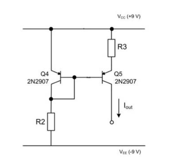
Homework Answers
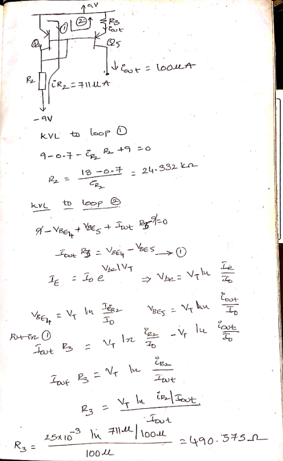
Add Answer to:
For the Widlar current mirror circuit shown below, design the
circuit to provide a current Iout=100µA,...
QUESTION 3 10 points Save Answer For the Widiar current mirror circuit shown below, design the...
 QUESTION 3 10 points Save Answer For the Widiar current mirror circuit shown below, design the circuit to provide a current lout=100μA, if R2-685 1A Hence, find the value of R3 (in Ω), given that VT-25mV. Voc (+9 V) R3 Q4 2N2907 Q5 2N2907 lout R2 VEE (-9 V)
Q2. For the op-amp circuit as shown below, given that RS = 49.5 k, RL =...
 Q2. For the op-amp circuit as shown below, given that RS = 49.5 k, RL = 12 k 2, R1 = 10 kO, R2 = 9 ㏀, R3 = 7.5 ko, R4 = 5 ㏀R5 = 2.2 k2 Ry vo Ry Ri Rs (a) Determine the voltage gain G1-vo1/vs: Submit Answer Tries o/5 (b) Determine the voltage gain G2-vo/vs: Submit Answer Tries o/5 Q3. For the op-amp circuit shown below, find the value of VO, where R1 = 20 Ω,...
Please answer clearly 2. Consider the circuit shown in Figure 1. Determine values of Ri, R2, and Rc to provide the quie...
 Please answer clearly
2. Consider the circuit shown in Figure 1. Determine values of Ri, R2, and Rc to provide the quiescent emitter current 1.5 mA and the quiescent collector to emitter voltage 5V. Assume β 100, Re-I㏀、Va= 200V, VBEon-0.7V, and VT= 25mV. R1 Rc Vcc に 10v R2 Re Figure 1: BJT biasing configuration
2. Consider the circuit shown in Figure 1. Determine values of Ri, R2, and Rc to provide the quiescent emitter current 1.5 mA and the...
Please answer clearly
2. Consider the circuit shown in Figure 1. Determine values of Ri, R2, and Rc to provide the quiescent emitter current 1.5 mA and the quiescent collector to emitter voltage 5V. Assume β 100, Re-I㏀、Va= 200V, VBEon-0.7V, and VT= 25mV. R1 Rc Vcc に 10v R2 Re Figure 1: BJT biasing configuration
2. Consider the circuit shown in Figure 1. Determine values of Ri, R2, and Rc to provide the quiescent emitter current 1.5 mA and the...
Recall the Offset Nulling Circuit that you used to zero out the offset of the LM741 OpAmp in L200...
 . please help me from a to
e
Recall the Offset Nulling Circuit that you used to zero out the offset of the LM741 OpAmp in L2002B, shown in Figure 1(a). An external 10 k2 potentiometer was applied across the emitter terminals of the current mirror formed by Q5 and Q6 in Figure 1(b), which can be thought of as making an adjustment to collector currents Ics and Ics such that Ics-Ics exactly A simplified version of that current mirror...
. please help me from a to
e
Recall the Offset Nulling Circuit that you used to zero out the offset of the LM741 OpAmp in L2002B, shown in Figure 1(a). An external 10 k2 potentiometer was applied across the emitter terminals of the current mirror formed by Q5 and Q6 in Figure 1(b), which can be thought of as making an adjustment to collector currents Ics and Ics such that Ics-Ics exactly A simplified version of that current mirror...
1. For the shown circuit with 2 electrical equipment (2 loads),
1. For the shown circuit with 2 electrical equipment (2 loads), R1 = 60 Ω R2 = 30 Ω ET = Vt = 120 V E: the potential difference in Volts Calculate the following: a) RT (total Resistance) b) IT (Total Current) c) IR1 (Current in equipment R1) d) IR2 (Current in equipment R2) e) VR2 (Voltage across R2) No circuit diagram was given. Just need the calculations from A - E.
Use the circuit diagram as shown in Figure A below to conduct the experiment and answer...
 Use the circuit diagram as shown in Figure A below to conduct the experiment and answer the questions 1 to 6. VCC VCC 15V 15V U2 5 3 + U1 741 Vouth R3 + Vouth 6 R1 741 2 1.Oko 2.2kg VEE -15V VEE -15V Vin= 0.75 V (PP) @ 2 kHz R2 R4 IH 4.7k02 10kΩ Figure A 1. Compute the theoretical Gain1 = -R2/R1 = ? 2. Compute the theoretical Gain2 = -R4/R3 = ? 3. Compute the...
Using Vtn=2V and kn= 0.150V/A, find R2, Vs2, and Vg2 which equals Vg1. 2.1.1 Design the...
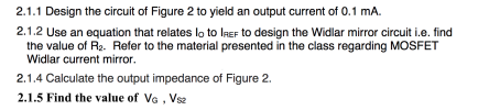 Using Vtn=2V and kn= 0.150V/A, find R2, Vs2, and Vg2 which
equals Vg1.
2.1.1 Design the circuit of Figure 2 to yield an output current of 0.1 mA. 2.1.2 Use an equation that relates lo to IREF to design the Widlar mirror circuit i.e. find the value of R2. Refer to the material presented in the class regarding MOSFET Widlar current mirror. 2.1.4 Calculate the output impedance of Figure 2. 2.1.5 Find the value of Va , Vs2 Vodi =...
Using Vtn=2V and kn= 0.150V/A, find R2, Vs2, and Vg2 which
equals Vg1.
2.1.1 Design the circuit of Figure 2 to yield an output current of 0.1 mA. 2.1.2 Use an equation that relates lo to IREF to design the Widlar mirror circuit i.e. find the value of R2. Refer to the material presented in the class regarding MOSFET Widlar current mirror. 2.1.4 Calculate the output impedance of Figure 2. 2.1.5 Find the value of Va , Vs2 Vodi =...
2. In the following current mirror circuit, Vcc -10V, and the three transistors, Q1, Q2, Q3, have...
 2. In the following current mirror circuit, Vcc -10V, and the three transistors, Q1, Q2, Q3, have the same saturation current (i.e.,IssIs), and with V for active mode is 0.7V. Then, the three beta values are given by: β91-100, ßQ2-50, and ßQ3-200. The thermal voltage is ντ-25mV. Assuming that you need an output current of i1mA: ref db (a) Find the collector, base, and emitter current for all three Q1 O2 transistors when ia 1mA. (b) Find the refern ie....
For the circuit shown below, let Vcc 9 V R2 RE-0.11 kQ, R1 3.6 k2. and R2 -5.6 kQ. The transistor parameters are β-200, VBE(on)-OTV, VA-100 V and VT = 0.026 V. (a) Determine the quiescent value o...
 For the circuit shown below, let Vcc 9 V R2 RE-0.11 kQ, R1 3.6 k2. and R2 -5.6 kQ. The transistor parameters are β-200, VBE(on)-OTV, VA-100 V and VT = 0.026 V. (a) Determine the quiescent value of IEQ (b) Find the small-signal voltage gain Av Vo/vs (c) Determine the output resistance R, looking into output terminals Av= 0.5589 Ro-0.4688 Ω Ro-0.9118 Ω leQ- 23.76 mA Ra " 0.6538 Ω leo 39.52 mA A, 0.9938
For the circuit shown below,...
For the circuit shown below, let Vcc 9 V R2 RE-0.11 kQ, R1 3.6 k2. and R2 -5.6 kQ. The transistor parameters are β-200, VBE(on)-OTV, VA-100 V and VT = 0.026 V. (a) Determine the quiescent value of IEQ (b) Find the small-signal voltage gain Av Vo/vs (c) Determine the output resistance R, looking into output terminals Av= 0.5589 Ro-0.4688 Ω Ro-0.9118 Ω leQ- 23.76 mA Ra " 0.6538 Ω leo 39.52 mA A, 0.9938
For the circuit shown below,...
A circuit that consists of 3 emf’s and 3 resistors as shown below. ε1=9 V, ε2=12...
 A circuit that consists of 3 emf’s and 3 resistors as shown
below. ε1=9 V, ε2=12 V, ε3=25 V and R1=5 Ω, R2 = 25 Ω and R3 =40
Ω
What is the value of the current flowing through
R2?
R2 R33 22
A circuit that consists of 3 emf’s and 3 resistors as shown
below. ε1=9 V, ε2=12 V, ε3=25 V and R1=5 Ω, R2 = 25 Ω and R3 =40
Ω
What is the value of the current flowing through
R2?
R2 R33 22
 QUESTION 3 10 points Save Answer For the Widiar current mirror circuit shown below, design the circuit to provide a current lout=100μA, if R2-685 1A Hence, find the value of R3 (in Ω), given that VT-25mV. Voc (+9 V) R3 Q4 2N2907 Q5 2N2907 lout R2 VEE (-9 V)
 Q2. For the op-amp circuit as shown below, given that RS = 49.5 k, RL = 12 k 2, R1 = 10 kO, R2 = 9 ㏀, R3 = 7.5 ko, R4 = 5 ㏀R5 = 2.2 k2 Ry vo Ry Ri Rs (a) Determine the voltage gain G1-vo1/vs: Submit Answer Tries o/5 (b) Determine the voltage gain G2-vo/vs: Submit Answer Tries o/5 Q3. For the op-amp circuit shown below, find the value of VO, where R1 = 20 Ω,...
 Please answer clearly
2. Consider the circuit shown in Figure 1. Determine values of Ri, R2, and Rc to provide the quiescent emitter current 1.5 mA and the quiescent collector to emitter voltage 5V. Assume β 100, Re-I㏀、Va= 200V, VBEon-0.7V, and VT= 25mV. R1 Rc Vcc に 10v R2 Re Figure 1: BJT biasing configuration
2. Consider the circuit shown in Figure 1. Determine values of Ri, R2, and Rc to provide the quiescent emitter current 1.5 mA and the...
Please answer clearly
2. Consider the circuit shown in Figure 1. Determine values of Ri, R2, and Rc to provide the quiescent emitter current 1.5 mA and the quiescent collector to emitter voltage 5V. Assume β 100, Re-I㏀、Va= 200V, VBEon-0.7V, and VT= 25mV. R1 Rc Vcc に 10v R2 Re Figure 1: BJT biasing configuration
2. Consider the circuit shown in Figure 1. Determine values of Ri, R2, and Rc to provide the quiescent emitter current 1.5 mA and the...
 . please help me from a to
e
Recall the Offset Nulling Circuit that you used to zero out the offset of the LM741 OpAmp in L2002B, shown in Figure 1(a). An external 10 k2 potentiometer was applied across the emitter terminals of the current mirror formed by Q5 and Q6 in Figure 1(b), which can be thought of as making an adjustment to collector currents Ics and Ics such that Ics-Ics exactly A simplified version of that current mirror...
. please help me from a to
e
Recall the Offset Nulling Circuit that you used to zero out the offset of the LM741 OpAmp in L2002B, shown in Figure 1(a). An external 10 k2 potentiometer was applied across the emitter terminals of the current mirror formed by Q5 and Q6 in Figure 1(b), which can be thought of as making an adjustment to collector currents Ics and Ics such that Ics-Ics exactly A simplified version of that current mirror...
 Use the circuit diagram as shown in Figure A below to conduct the experiment and answer the questions 1 to 6. VCC VCC 15V 15V U2 5 3 + U1 741 Vouth R3 + Vouth 6 R1 741 2 1.Oko 2.2kg VEE -15V VEE -15V Vin= 0.75 V (PP) @ 2 kHz R2 R4 IH 4.7k02 10kΩ Figure A 1. Compute the theoretical Gain1 = -R2/R1 = ? 2. Compute the theoretical Gain2 = -R4/R3 = ? 3. Compute the...
 Using Vtn=2V and kn= 0.150V/A, find R2, Vs2, and Vg2 which
equals Vg1.
2.1.1 Design the circuit of Figure 2 to yield an output current of 0.1 mA. 2.1.2 Use an equation that relates lo to IREF to design the Widlar mirror circuit i.e. find the value of R2. Refer to the material presented in the class regarding MOSFET Widlar current mirror. 2.1.4 Calculate the output impedance of Figure 2. 2.1.5 Find the value of Va , Vs2 Vodi =...
Using Vtn=2V and kn= 0.150V/A, find R2, Vs2, and Vg2 which
equals Vg1.
2.1.1 Design the circuit of Figure 2 to yield an output current of 0.1 mA. 2.1.2 Use an equation that relates lo to IREF to design the Widlar mirror circuit i.e. find the value of R2. Refer to the material presented in the class regarding MOSFET Widlar current mirror. 2.1.4 Calculate the output impedance of Figure 2. 2.1.5 Find the value of Va , Vs2 Vodi =...
 2. In the following current mirror circuit, Vcc -10V, and the three transistors, Q1, Q2, Q3, have the same saturation current (i.e.,IssIs), and with V for active mode is 0.7V. Then, the three beta values are given by: β91-100, ßQ2-50, and ßQ3-200. The thermal voltage is ντ-25mV. Assuming that you need an output current of i1mA: ref db (a) Find the collector, base, and emitter current for all three Q1 O2 transistors when ia 1mA. (b) Find the refern ie....
 For the circuit shown below, let Vcc 9 V R2 RE-0.11 kQ, R1 3.6 k2. and R2 -5.6 kQ. The transistor parameters are β-200, VBE(on)-OTV, VA-100 V and VT = 0.026 V. (a) Determine the quiescent value of IEQ (b) Find the small-signal voltage gain Av Vo/vs (c) Determine the output resistance R, looking into output terminals Av= 0.5589 Ro-0.4688 Ω Ro-0.9118 Ω leQ- 23.76 mA Ra " 0.6538 Ω leo 39.52 mA A, 0.9938
For the circuit shown below,...
For the circuit shown below, let Vcc 9 V R2 RE-0.11 kQ, R1 3.6 k2. and R2 -5.6 kQ. The transistor parameters are β-200, VBE(on)-OTV, VA-100 V and VT = 0.026 V. (a) Determine the quiescent value of IEQ (b) Find the small-signal voltage gain Av Vo/vs (c) Determine the output resistance R, looking into output terminals Av= 0.5589 Ro-0.4688 Ω Ro-0.9118 Ω leQ- 23.76 mA Ra " 0.6538 Ω leo 39.52 mA A, 0.9938
For the circuit shown below,...
 A circuit that consists of 3 emf’s and 3 resistors as shown
below. ε1=9 V, ε2=12 V, ε3=25 V and R1=5 Ω, R2 = 25 Ω and R3 =40
Ω
What is the value of the current flowing through
R2?
R2 R33 22
A circuit that consists of 3 emf’s and 3 resistors as shown
below. ε1=9 V, ε2=12 V, ε3=25 V and R1=5 Ω, R2 = 25 Ω and R3 =40
Ω
What is the value of the current flowing through
R2?
R2 R33 22
Most questions answered within 3 hours.
-
Where is the error in this code sequence?
String s1 = "Hello";
String s2 = "ello";...
asked 11 months ago -
Financial data for Joel de Paris, Inc., for last year
follow:
Joel de Paris, Inc.
Balance...
asked 11 months ago -
Consider this reaction:
Al2(SO4)3 (aq)+ BaCl3
(aq) Al2Cl6 (aq)- +
3BaSO4(s) . What is the...
asked 11 months ago -
Suppose that Savneet is considering increasing her
recent random sample from 20 car rentals to 40...
asked 11 months ago -
Trucks arrive at an unloading terminal at an average rate of 120
per hour.
Trucks arrive...
asked 11 months ago -
Why are methanol and ethanol completely soluble in water while
octanol is not very little soluble....
asked 11 months ago -
A facilities manager at a university reads in a research report
that the mean amount of...
asked 11 months ago -
When the CuSO4 is rehydrated by adding water to the anhydrous
compound, is this an endothermic...
asked 11 months ago -
A ray of sunlight is passing from diamond into crown glass; the
angle of incidence is...
asked 11 months ago -
A block of mass 0.249 kg is placed on top of a light, vertical
spring of...
asked 11 months ago -
how do the kidneys compensate in the presences of acidosis
a) trigger hyperventilate
b) reserve acid...
asked 11 months ago -
Question 501 pts
The rental rate of capital to the firm increases. Which of the
following...
asked 11 months ago