 PLEASE SHOW WORK
Homework Answers


Add Answer to:
PLEASE SHOW WORK
The circuit shown at the bottom is intended to be a gated latch...
a) (5 marks) Explain the difference between a latch, a gated latch and a flip flop....
 a) (5 marks) Explain the difference between a latch, a gated latch and a flip flop. b) (5 marks) A gated SR latch has the following schematic diagram CLK a) Draw a timing diagram showing the Q and Q outputs for the following sequence of inputs: CLK R Assume that the initial state of the outputs is Q 0 and Q 1 c) (5 marks) Draw a schematic diagram for a rising edge-triggered master-slave D flip- flop built using two...
(a) A negative-level sensitive (negative triggered) D latch circuit can be designed using a circuit as...
 (a) A negative-level sensitive (negative triggered) D latch circuit can be designed using a circuit as shown in Figure 3 CLK DH CLK ola CLK Figure 3 Obtain the equation for the output of the circuit, Q. Analyse the circuit and determine when the circuit is in 'transparent form and "opaque' form with regards to the clock input. Assess the output at these two forms. (ii) Modify the circuit to produce a positive-level sensitive (positive triggered) D latch. Draw and...
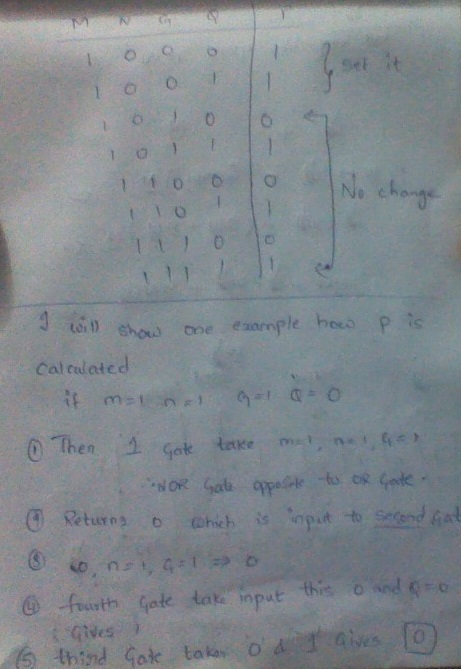
2. Answer the following questions about the circuit shown below, which differs slightly from the Gated...
 2. Answer the following questions about the circuit shown below, which differs slightly from the Gated SR NOR Latch discussed before due to having NOR gates instead of AND gates. a. (20 points) What input combinations for S, R, and G will not change the output of the circuit (that is, which input corresponds to the output having no change) b. (10 points) What input combinations for S, R, and G will produce an undesirable output?
please answer all thanks very much! Question 3 Shown below is a schematic diagram of a...
 please answer all thanks very much!
Question 3 Shown below is a schematic diagram of a counter made up of three JK flip-flops. (d) Shown below is a master-slave D flip-flop. This is made using two gated D latches. The truth table for a gated D latch is also shown below. HIGH J J CLK ас ас ac Truth table: gated D latch D EN D D, Q. D, 0. 0 0 go CLK ΕΝΟ ENO: 0 0 1 0...
please answer all thanks very much!
Question 3 Shown below is a schematic diagram of a counter made up of three JK flip-flops. (d) Shown below is a master-slave D flip-flop. This is made using two gated D latches. The truth table for a gated D latch is also shown below. HIGH J J CLK ас ас ac Truth table: gated D latch D EN D D, Q. D, 0. 0 0 go CLK ΕΝΟ ENO: 0 0 1 0...
can anyone slove this.Thank you. PROBLEM 2: In the circuit shown, A is a D-type latch...
 can anyone slove this.Thank you.
PROBLEM 2: In the circuit shown, A is a D-type latch and B is a D-type flip flop. For the input waveforms given for the clock signal (Clk) and the input X, accurately draw the resulting waveforms at outputs QA and QB Assume that both Q and Quare initially at 0. X D QH A CIK 22 Clk х D Q B QA DC Qв Draw QA and QB or scan and paste your hand...
can anyone slove this.Thank you.
PROBLEM 2: In the circuit shown, A is a D-type latch and B is a D-type flip flop. For the input waveforms given for the clock signal (Clk) and the input X, accurately draw the resulting waveforms at outputs QA and QB Assume that both Q and Quare initially at 0. X D QH A CIK 22 Clk х D Q B QA DC Qв Draw QA and QB or scan and paste your hand...
Please show all work The de-de converter shown in Fig. 1 operates in continuous conduction mode....
 Please show all work
The de-de converter shown in Fig. 1 operates in continuous conduction mode. Assume that all components are ideal. a) Draw the small-signal ac equivalent circuit. b) Assuming that the duty cycle is held constant (i.e. d-0), derive the input-to- output transfer function v (s) 1) Make sure to show your steps. Ru Fig. 1
Please show all work
The de-de converter shown in Fig. 1 operates in continuous conduction mode. Assume that all components are ideal. a) Draw the small-signal ac equivalent circuit. b) Assuming that the duty cycle is held constant (i.e. d-0), derive the input-to- output transfer function v (s) 1) Make sure to show your steps. Ru Fig. 1
Please show work! Homework Assignment 1 You must show all your work to earn points ECON...
 Please show work!
Homework Assignment 1 You must show all your work to earn points ECON 3125 SP19 Name: 1. Use the graph below to answer the questions: 80 70 50 40 30 20 10 State the equation for the demand curve (inverse demand function) shown in the graph above using the format P.-a-bQ a. b. State the equation for the demand function implied in the graph using the format Q.-c-dP c. Find the equation for Total Revenue, where TR...
Please show work!
Homework Assignment 1 You must show all your work to earn points ECON 3125 SP19 Name: 1. Use the graph below to answer the questions: 80 70 50 40 30 20 10 State the equation for the demand curve (inverse demand function) shown in the graph above using the format P.-a-bQ a. b. State the equation for the demand function implied in the graph using the format Q.-c-dP c. Find the equation for Total Revenue, where TR...
NAND Problem 3 (30 points) Consider the circuit shown alongside. Notice that there is one A input...
 NAND Problem 3 (30 points) Consider the circuit shown alongside. Notice that there is one A input x and one output. FULL ADDER XOR (a) [5 points] Determine the B Q Cout Clk flip-flop input equations and xin the output z in terms of the present states A, B and input variable x in other words 4-1 compute T, J, K and z. MUX (b) [10 points] Use the above 1 equations to derive the state- 01 table. Assume the...
Please solve the two problems shown and show work. thank you! 5) In the following circuit...
 Please solve the two problems shown and show work.
thank you!
5) In the following circuit find an equation for v(t) the voltage across the capacitor for t>O. You may assume the circuit is in the steady-state just before the switch opens at t-0. 6 N 50 -Mu IH 3 10 ml Add equation 6) For the following circuit find an equation for v(t) fort > 0. You can assume that the circuit had reached the steady-state condition before the...
Please solve the two problems shown and show work.
thank you!
5) In the following circuit find an equation for v(t) the voltage across the capacitor for t>O. You may assume the circuit is in the steady-state just before the switch opens at t-0. 6 N 50 -Mu IH 3 10 ml Add equation 6) For the following circuit find an equation for v(t) fort > 0. You can assume that the circuit had reached the steady-state condition before the...
A sequential circuit has one flip-flop Q, two inputs x and y, and one output. It consists of a full-adder circuit connected to a D flip-flop, as shown in Figure 1 as follows.
 A sequential circuit has one flip-flop Q, two inputs x and y, and one output. It consists of a full-adder circuit connected to a D flip-flop, as shown in Figure 1 as follows. For the sequential circuit derive (or draw) the,A) state equation B) state table C) state diagram
 a) (5 marks) Explain the difference between a latch, a gated latch and a flip flop. b) (5 marks) A gated SR latch has the following schematic diagram CLK a) Draw a timing diagram showing the Q and Q outputs for the following sequence of inputs: CLK R Assume that the initial state of the outputs is Q 0 and Q 1 c) (5 marks) Draw a schematic diagram for a rising edge-triggered master-slave D flip- flop built using two...
 (a) A negative-level sensitive (negative triggered) D latch circuit can be designed using a circuit as shown in Figure 3 CLK DH CLK ola CLK Figure 3 Obtain the equation for the output of the circuit, Q. Analyse the circuit and determine when the circuit is in 'transparent form and "opaque' form with regards to the clock input. Assess the output at these two forms. (ii) Modify the circuit to produce a positive-level sensitive (positive triggered) D latch. Draw and...
 2. Answer the following questions about the circuit shown below, which differs slightly from the Gated SR NOR Latch discussed before due to having NOR gates instead of AND gates. a. (20 points) What input combinations for S, R, and G will not change the output of the circuit (that is, which input corresponds to the output having no change) b. (10 points) What input combinations for S, R, and G will produce an undesirable output?
 please answer all thanks very much!
Question 3 Shown below is a schematic diagram of a counter made up of three JK flip-flops. (d) Shown below is a master-slave D flip-flop. This is made using two gated D latches. The truth table for a gated D latch is also shown below. HIGH J J CLK ас ас ac Truth table: gated D latch D EN D D, Q. D, 0. 0 0 go CLK ΕΝΟ ENO: 0 0 1 0...
please answer all thanks very much!
Question 3 Shown below is a schematic diagram of a counter made up of three JK flip-flops. (d) Shown below is a master-slave D flip-flop. This is made using two gated D latches. The truth table for a gated D latch is also shown below. HIGH J J CLK ас ас ac Truth table: gated D latch D EN D D, Q. D, 0. 0 0 go CLK ΕΝΟ ENO: 0 0 1 0...
 can anyone slove this.Thank you.
PROBLEM 2: In the circuit shown, A is a D-type latch and B is a D-type flip flop. For the input waveforms given for the clock signal (Clk) and the input X, accurately draw the resulting waveforms at outputs QA and QB Assume that both Q and Quare initially at 0. X D QH A CIK 22 Clk х D Q B QA DC Qв Draw QA and QB or scan and paste your hand...
can anyone slove this.Thank you.
PROBLEM 2: In the circuit shown, A is a D-type latch and B is a D-type flip flop. For the input waveforms given for the clock signal (Clk) and the input X, accurately draw the resulting waveforms at outputs QA and QB Assume that both Q and Quare initially at 0. X D QH A CIK 22 Clk х D Q B QA DC Qв Draw QA and QB or scan and paste your hand...
 Please show all work
The de-de converter shown in Fig. 1 operates in continuous conduction mode. Assume that all components are ideal. a) Draw the small-signal ac equivalent circuit. b) Assuming that the duty cycle is held constant (i.e. d-0), derive the input-to- output transfer function v (s) 1) Make sure to show your steps. Ru Fig. 1
Please show all work
The de-de converter shown in Fig. 1 operates in continuous conduction mode. Assume that all components are ideal. a) Draw the small-signal ac equivalent circuit. b) Assuming that the duty cycle is held constant (i.e. d-0), derive the input-to- output transfer function v (s) 1) Make sure to show your steps. Ru Fig. 1
 Please show work!
Homework Assignment 1 You must show all your work to earn points ECON 3125 SP19 Name: 1. Use the graph below to answer the questions: 80 70 50 40 30 20 10 State the equation for the demand curve (inverse demand function) shown in the graph above using the format P.-a-bQ a. b. State the equation for the demand function implied in the graph using the format Q.-c-dP c. Find the equation for Total Revenue, where TR...
Please show work!
Homework Assignment 1 You must show all your work to earn points ECON 3125 SP19 Name: 1. Use the graph below to answer the questions: 80 70 50 40 30 20 10 State the equation for the demand curve (inverse demand function) shown in the graph above using the format P.-a-bQ a. b. State the equation for the demand function implied in the graph using the format Q.-c-dP c. Find the equation for Total Revenue, where TR...
 NAND Problem 3 (30 points) Consider the circuit shown alongside. Notice that there is one A input x and one output. FULL ADDER XOR (a) [5 points] Determine the B Q Cout Clk flip-flop input equations and xin the output z in terms of the present states A, B and input variable x in other words 4-1 compute T, J, K and z. MUX (b) [10 points] Use the above 1 equations to derive the state- 01 table. Assume the...
 Please solve the two problems shown and show work.
thank you!
5) In the following circuit find an equation for v(t) the voltage across the capacitor for t>O. You may assume the circuit is in the steady-state just before the switch opens at t-0. 6 N 50 -Mu IH 3 10 ml Add equation 6) For the following circuit find an equation for v(t) fort > 0. You can assume that the circuit had reached the steady-state condition before the...
Please solve the two problems shown and show work.
thank you!
5) In the following circuit find an equation for v(t) the voltage across the capacitor for t>O. You may assume the circuit is in the steady-state just before the switch opens at t-0. 6 N 50 -Mu IH 3 10 ml Add equation 6) For the following circuit find an equation for v(t) fort > 0. You can assume that the circuit had reached the steady-state condition before the...
 A sequential circuit has one flip-flop Q, two inputs x and y, and one output. It consists of a full-adder circuit connected to a D flip-flop, as shown in Figure 1 as follows. For the sequential circuit derive (or draw) the,A) state equation B) state table C) state diagram
Most questions answered within 3 hours.
-
Where is the error in this code sequence?
String s1 = "Hello";
String s2 = "ello";...
asked 10 months ago -
Financial data for Joel de Paris, Inc., for last year
follow:
Joel de Paris, Inc.
Balance...
asked 10 months ago -
Consider this reaction:
Al2(SO4)3 (aq)+ BaCl3
(aq) Al2Cl6 (aq)- +
3BaSO4(s) . What is the...
asked 10 months ago -
Suppose that Savneet is considering increasing her
recent random sample from 20 car rentals to 40...
asked 10 months ago -
Trucks arrive at an unloading terminal at an average rate of 120
per hour.
Trucks arrive...
asked 10 months ago -
Why are methanol and ethanol completely soluble in water while
octanol is not very little soluble....
asked 10 months ago -
A facilities manager at a university reads in a research report
that the mean amount of...
asked 10 months ago -
When the CuSO4 is rehydrated by adding water to the anhydrous
compound, is this an endothermic...
asked 10 months ago -
A ray of sunlight is passing from diamond into crown glass; the
angle of incidence is...
asked 10 months ago -
A block of mass 0.249 kg is placed on top of a light, vertical
spring of...
asked 10 months ago -
how do the kidneys compensate in the presences of acidosis
a) trigger hyperventilate
b) reserve acid...
asked 10 months ago -
Question 501 pts
The rental rate of capital to the firm increases. Which of the
following...
asked 10 months ago