
Homework Answers
Add Answer to:
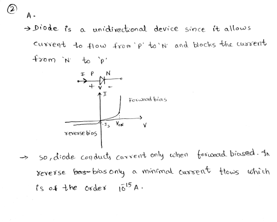
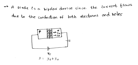
A. Explain the following statements with regards to PN junction Diode with proper diagrams to illustrate...
3 A. Define Built in Potential in a PN Junction. With the help of diagrams explain...
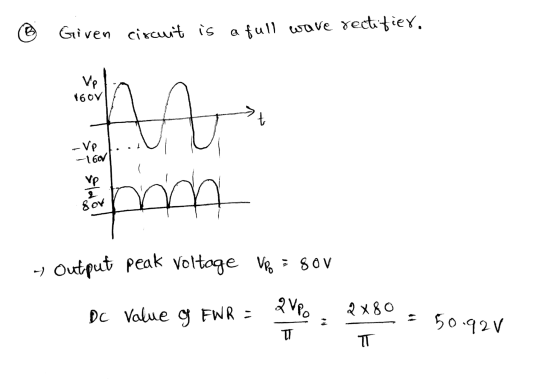
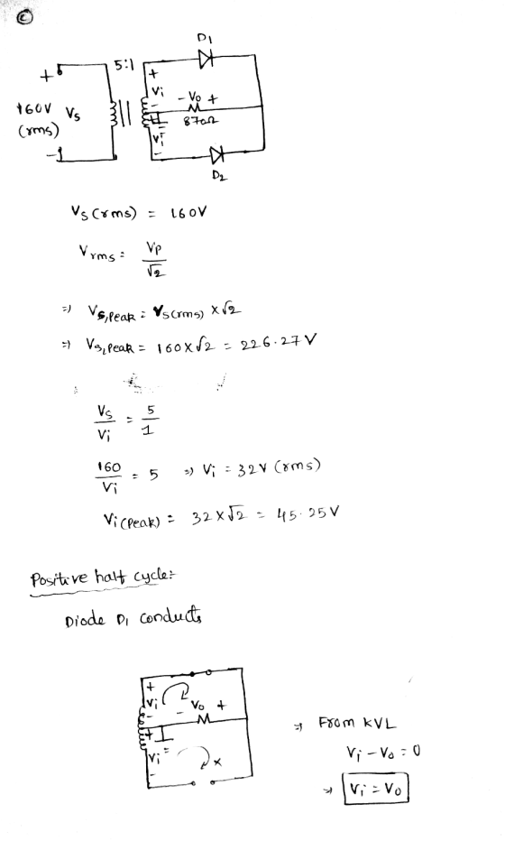
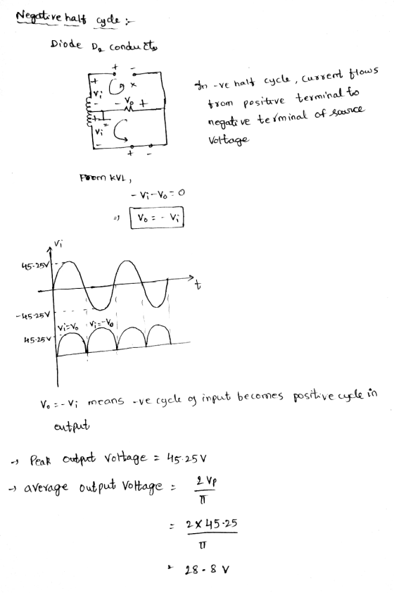
 3 A. Define Built in Potential in a PN Junction. With the help of diagrams explain how the built in potential is formed when no external bias is applied [2 marks] B. A rectifier circuit with four silicon diodes and the output frequency equal to twice of the input frequency. The input peak to peak voltage Vin pp = 25V, the load resistance R = 560 12. [3 marks) a. Name the circuit b. Draw the circuit diagram c. Explain...
Fral Assignment (a) Draw the circuit diagram a Centre tapped Pull Wave Rectifier using a 1000-500...
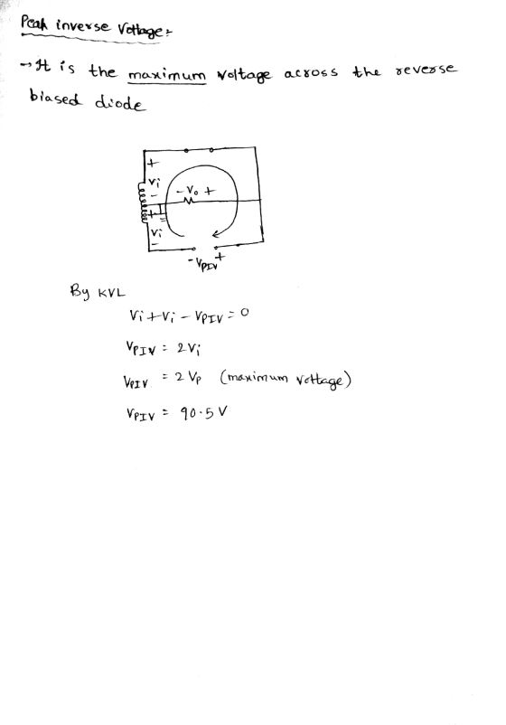
 Fral Assignment (a) Draw the circuit diagram a Centre tapped Pull Wave Rectifier using a 1000-500 Centre tapped Transformer. Assume a signal of 24 V, 50 Hz at the primary of the transformer Assume silicon diodes. Find: (11) Peak Output Voltage, Volt RMS Output Voltage, Vor). the peak inverse voltage [3 Mark) (b) Find the current flowing through the R1,R2,R3 and R4 and Vx. If Vs=15v,RI-2K22,R2-26092, R3=1.122 and R4-60002. (1) Assuming Ideal diode (2) Si diode (3) Ge diode [3...
The parameters of a pn junction diode at 300K are listed in the following table, the...
 The parameters of a pn junction diode at 300K are listed in the following table, the cross section area of the junction is 105 cm2 n region N10" cm Hu = 850 cm?/V-s p region t,e = 10-6 s ,1" 1250 cm2/V-s 11,-420 cm2/V-s 320 cm/V-s (a) Sketch a band diagram at equilibrium (b) Find the reserve saturation current (c) Find the ideal diode current with forward bias voltage at 0.5 V and 0.7 V, respectively. (d) Find the current...
A silicon PN junction diode is constructed using N-type silicon in which the Fermi level is...
 A silicon PN junction diode is constructed using N-type silicon in which the Fermi level is 100 meV below the conduction band edge and P-type silicon in which the Fermi level is 120 meV above the valence band edge a) What are the majority and minority carrier concentrations on each side of the junction under thermal equilibrium? b) What is the value of the built-in voltage? c) Determine the width of the depletion region on both sides of the junction...
do appreciate the process in details and neat (b) The circuit shown in Figure 2 utilizes two diodes, Di and D2, a R, resistor R1 = 10 Ω. Assume a piecewise linear (PWL) model for the diode that ha...
 do appreciate the process in details and neat
(b) The circuit shown in Figure 2 utilizes two diodes, Di and D2, a R, resistor R1 = 10 Ω. Assume a piecewise linear (PWL) model for the diode that has VD 07 and r-5 Ω. Draw the output voltage, vo, as function of the input voltage, Vin, characteristics of this circuit at point assuming the input voltage has a peak-to-peak voltage of 3 Volt. There is no need to draw the...
do appreciate the process in details and neat
(b) The circuit shown in Figure 2 utilizes two diodes, Di and D2, a R, resistor R1 = 10 Ω. Assume a piecewise linear (PWL) model for the diode that has VD 07 and r-5 Ω. Draw the output voltage, vo, as function of the input voltage, Vin, characteristics of this circuit at point assuming the input voltage has a peak-to-peak voltage of 3 Volt. There is no need to draw the...
Consider a 4-diode bridge rectifier that rectifies a +-240V square wave within a UPS. For now,...
 Consider a 4-diode bridge rectifier that rectifies a +-240V square wave within a UPS. For now, assume a 100-ohm resistive load and draw the circuit. Model the forward characteristics of each diode with an on-voltage of 0.5 volt plus an internal resistance of 1 ohm. Model the reverse (leakage) characteristics of each diode as ideal. Draw tidy graphs of the input, output as well as (NB careful!) diode voltages. Show calculations to obtain graph values. Also draw tidy graphs of...
Please note that D4 is the one that was destroyed not D1. Please I posted this but they answer it...
 Please note that D4 is the one that was destroyed not D1.
Please I posted this but they answer it differently
QUESTION (2) Due to an abnormal operating condition, Diode D4 in this full-wave rectifier circuit was suddenly destroyed, and stopped Vconducting in both forward and reverse directions (i.e. open circuit) C- R Assume that all other diodes are ideal with zero forward voltage drop and that the time constant RC- 5 ms. stt) 10V For a 1 kHz triangular...
Please note that D4 is the one that was destroyed not D1.
Please I posted this but they answer it differently
QUESTION (2) Due to an abnormal operating condition, Diode D4 in this full-wave rectifier circuit was suddenly destroyed, and stopped Vconducting in both forward and reverse directions (i.e. open circuit) C- R Assume that all other diodes are ideal with zero forward voltage drop and that the time constant RC- 5 ms. stt) 10V For a 1 kHz triangular...
VOLTAGE-DIVIDER BIAS 179 CONFIGURATION h determined in Example 4.7. Essentially, exact and approx...
 VOLTAGE-DIVIDER BIAS 179 CONFIGURATION h determined in Example 4.7. Essentially, exact and approximate techniques is the ten the 07 step down transformer and a load RL of 820 ohms. It is connected to an ac source of 100 VAC rms, 50 Hz. (hint: note the rms values, and for diode PIV, assume ideal diodes and draw the PIV eqv ckts) ve rectifier circuit has a 10:1 3. A positive output, a. Draw this circuit.. b. Find Vp and Vave at...
In Figure 9, the transformer primary voltage is 120V and step-downratiois 10:1 Assume the practical diode...
 In Figure 9, the transformer primary voltage is 120V and step-downratiois 10:1 Assume the practical diode model. 9. a) i) Name the type of circuit (1 mark) Determine the peak output voltage, Volout) (4 marks) iiI What is the PIV rating required for the diodes (2 marks) D, D3 120 V psecy R Plout) 10 k2 DA Figure 9 b) A certain power supply filter produces an output with a ripple of 100mV peak-to- peak and a dc value of...
Design a FULL WAVE BRIDGE RECTIFIER circuit that will: Take 120volts ac, 60 hz, sinusoidal waveform...
 Design a FULL WAVE BRIDGE RECTIFIER circuit that will:
Take 120volts ac, 60 hz, sinusoidal waveform and convert
it to a “regulated “dc value
giving 12 volts +, - 1 volt across a 2000-ohm output
load resistor with no more than 2%
ripple voltage.
You may assume:
a. An ideal power transformer as discussed in class.
b. For hand computations, you must assume a diode given by
Figure 4.8 page 185.
c. A filter capacitor sized per the textbook equation...
Design a FULL WAVE BRIDGE RECTIFIER circuit that will:
Take 120volts ac, 60 hz, sinusoidal waveform and convert
it to a “regulated “dc value
giving 12 volts +, - 1 volt across a 2000-ohm output
load resistor with no more than 2%
ripple voltage.
You may assume:
a. An ideal power transformer as discussed in class.
b. For hand computations, you must assume a diode given by
Figure 4.8 page 185.
c. A filter capacitor sized per the textbook equation...
 3 A. Define Built in Potential in a PN Junction. With the help of diagrams explain how the built in potential is formed when no external bias is applied [2 marks] B. A rectifier circuit with four silicon diodes and the output frequency equal to twice of the input frequency. The input peak to peak voltage Vin pp = 25V, the load resistance R = 560 12. [3 marks) a. Name the circuit b. Draw the circuit diagram c. Explain...
 Fral Assignment (a) Draw the circuit diagram a Centre tapped Pull Wave Rectifier using a 1000-500 Centre tapped Transformer. Assume a signal of 24 V, 50 Hz at the primary of the transformer Assume silicon diodes. Find: (11) Peak Output Voltage, Volt RMS Output Voltage, Vor). the peak inverse voltage [3 Mark) (b) Find the current flowing through the R1,R2,R3 and R4 and Vx. If Vs=15v,RI-2K22,R2-26092, R3=1.122 and R4-60002. (1) Assuming Ideal diode (2) Si diode (3) Ge diode [3...
 The parameters of a pn junction diode at 300K are listed in the following table, the cross section area of the junction is 105 cm2 n region N10" cm Hu = 850 cm?/V-s p region t,e = 10-6 s ,1" 1250 cm2/V-s 11,-420 cm2/V-s 320 cm/V-s (a) Sketch a band diagram at equilibrium (b) Find the reserve saturation current (c) Find the ideal diode current with forward bias voltage at 0.5 V and 0.7 V, respectively. (d) Find the current...
 A silicon PN junction diode is constructed using N-type silicon in which the Fermi level is 100 meV below the conduction band edge and P-type silicon in which the Fermi level is 120 meV above the valence band edge a) What are the majority and minority carrier concentrations on each side of the junction under thermal equilibrium? b) What is the value of the built-in voltage? c) Determine the width of the depletion region on both sides of the junction...
 do appreciate the process in details and neat
(b) The circuit shown in Figure 2 utilizes two diodes, Di and D2, a R, resistor R1 = 10 Ω. Assume a piecewise linear (PWL) model for the diode that has VD 07 and r-5 Ω. Draw the output voltage, vo, as function of the input voltage, Vin, characteristics of this circuit at point assuming the input voltage has a peak-to-peak voltage of 3 Volt. There is no need to draw the...
do appreciate the process in details and neat
(b) The circuit shown in Figure 2 utilizes two diodes, Di and D2, a R, resistor R1 = 10 Ω. Assume a piecewise linear (PWL) model for the diode that has VD 07 and r-5 Ω. Draw the output voltage, vo, as function of the input voltage, Vin, characteristics of this circuit at point assuming the input voltage has a peak-to-peak voltage of 3 Volt. There is no need to draw the...
 Consider a 4-diode bridge rectifier that rectifies a +-240V square wave within a UPS. For now, assume a 100-ohm resistive load and draw the circuit. Model the forward characteristics of each diode with an on-voltage of 0.5 volt plus an internal resistance of 1 ohm. Model the reverse (leakage) characteristics of each diode as ideal. Draw tidy graphs of the input, output as well as (NB careful!) diode voltages. Show calculations to obtain graph values. Also draw tidy graphs of...
 Please note that D4 is the one that was destroyed not D1.
Please I posted this but they answer it differently
QUESTION (2) Due to an abnormal operating condition, Diode D4 in this full-wave rectifier circuit was suddenly destroyed, and stopped Vconducting in both forward and reverse directions (i.e. open circuit) C- R Assume that all other diodes are ideal with zero forward voltage drop and that the time constant RC- 5 ms. stt) 10V For a 1 kHz triangular...
Please note that D4 is the one that was destroyed not D1.
Please I posted this but they answer it differently
QUESTION (2) Due to an abnormal operating condition, Diode D4 in this full-wave rectifier circuit was suddenly destroyed, and stopped Vconducting in both forward and reverse directions (i.e. open circuit) C- R Assume that all other diodes are ideal with zero forward voltage drop and that the time constant RC- 5 ms. stt) 10V For a 1 kHz triangular...
 VOLTAGE-DIVIDER BIAS 179 CONFIGURATION h determined in Example 4.7. Essentially, exact and approximate techniques is the ten the 07 step down transformer and a load RL of 820 ohms. It is connected to an ac source of 100 VAC rms, 50 Hz. (hint: note the rms values, and for diode PIV, assume ideal diodes and draw the PIV eqv ckts) ve rectifier circuit has a 10:1 3. A positive output, a. Draw this circuit.. b. Find Vp and Vave at...
 In Figure 9, the transformer primary voltage is 120V and step-downratiois 10:1 Assume the practical diode model. 9. a) i) Name the type of circuit (1 mark) Determine the peak output voltage, Volout) (4 marks) iiI What is the PIV rating required for the diodes (2 marks) D, D3 120 V psecy R Plout) 10 k2 DA Figure 9 b) A certain power supply filter produces an output with a ripple of 100mV peak-to- peak and a dc value of...
 Design a FULL WAVE BRIDGE RECTIFIER circuit that will:
Take 120volts ac, 60 hz, sinusoidal waveform and convert
it to a “regulated “dc value
giving 12 volts +, - 1 volt across a 2000-ohm output
load resistor with no more than 2%
ripple voltage.
You may assume:
a. An ideal power transformer as discussed in class.
b. For hand computations, you must assume a diode given by
Figure 4.8 page 185.
c. A filter capacitor sized per the textbook equation...
Design a FULL WAVE BRIDGE RECTIFIER circuit that will:
Take 120volts ac, 60 hz, sinusoidal waveform and convert
it to a “regulated “dc value
giving 12 volts +, - 1 volt across a 2000-ohm output
load resistor with no more than 2%
ripple voltage.
You may assume:
a. An ideal power transformer as discussed in class.
b. For hand computations, you must assume a diode given by
Figure 4.8 page 185.
c. A filter capacitor sized per the textbook equation...
Most questions answered within 3 hours.
-
Where is the error in this code sequence?
String s1 = "Hello";
String s2 = "ello";...
asked 11 months ago -
Financial data for Joel de Paris, Inc., for last year
follow:
Joel de Paris, Inc.
Balance...
asked 11 months ago -
Consider this reaction:
Al2(SO4)3 (aq)+ BaCl3
(aq) Al2Cl6 (aq)- +
3BaSO4(s) . What is the...
asked 11 months ago -
Suppose that Savneet is considering increasing her
recent random sample from 20 car rentals to 40...
asked 11 months ago -
Trucks arrive at an unloading terminal at an average rate of 120
per hour.
Trucks arrive...
asked 11 months ago -
Why are methanol and ethanol completely soluble in water while
octanol is not very little soluble....
asked 11 months ago -
A facilities manager at a university reads in a research report
that the mean amount of...
asked 11 months ago -
When the CuSO4 is rehydrated by adding water to the anhydrous
compound, is this an endothermic...
asked 11 months ago -
A ray of sunlight is passing from diamond into crown glass; the
angle of incidence is...
asked 11 months ago -
A block of mass 0.249 kg is placed on top of a light, vertical
spring of...
asked 11 months ago -
how do the kidneys compensate in the presences of acidosis
a) trigger hyperventilate
b) reserve acid...
asked 11 months ago -
Question 501 pts
The rental rate of capital to the firm increases. Which of the
following...
asked 11 months ago