
Homework Answers


Add Answer to:
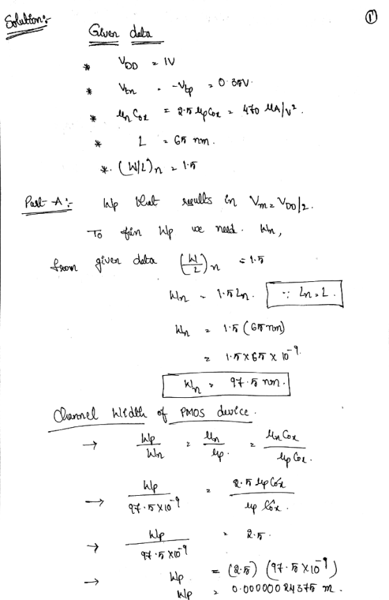
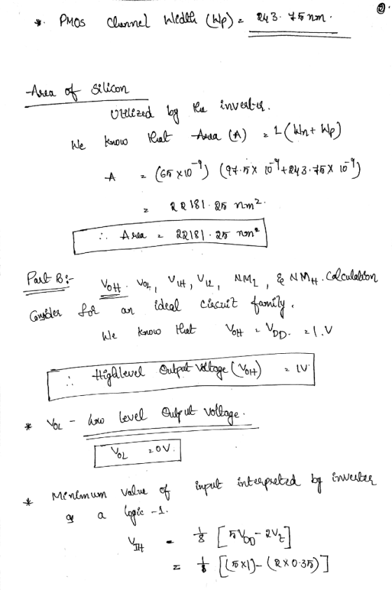
14.31 Consider a CMOS inverter fabricated in a 65-nm CMOS process for which VopV, V 0.35...
Section 14.3: The CMOS Inverter 14.31 Consider a CMOS inverter fabricated in a 65-nm CMOS process...
 Section 14.3: The CMOS Inverter 14.31 Consider a CMOS inverter fabricated in a 65-nm CMOS process for which VppV, VVp 0.35 V, and ?? Car-2.5MyCar-470 ??/V'. In addition, QN and QP have L = 65 nm and (WIL), 1.5. (a) Find W, that results in V Vpp/2. What is the silicon area utilized by the inverter in this case? (b) For the matched case in (a), find the values of Vo, VoL ,VIL, NM,, and NM (c) For the matched...
14.31 Consider a CMOS inverter fabricated in a 65-nm CMOS process for which Vpp = 1V,...
 14.31 Consider a CMOS inverter fabricated in a 65-nm CMOS process for which Vpp = 1V, V = - = 0.35 V, and u C = 2.54 C = 470 HA/V'. In addition, ex and Q, have L = 65 nm and (WIL), = 1.5. (a) Find W that results in V = V 2. What is the silicon area utilized by the inverter in this case? (b) For the matched case in (a), find the values of Vow, VOL...
Problem 1 A matched CMOS inverter fabricated in a process for which Cor 3.7 fFjum2, μnCz-180...
 Problem 1 A matched CMOS inverter fabricated in a process for which Cor 3.7 fFjum2, μnCz-180 μ A/V2, tlpCor = 45 μA/V2. Itn--It,- = 3.3 V, uses W, 0.75 μrm and Ln-Lpー0.5,nn. The overlap capacitance and the effective drain-body capacitance per micrometer of gate width are 0.4 fF and 1.0 fF, respectively. The wiring capacitance is Cu2 fF. If the inverter is driving another identical inverter, find tPLH, tPH L, and tp. For how much additional capacitance load does the...
19. Consider the CMOS inverter below with VDo-5.0 V and device parameters: p-channel K--2.5mA/V2, Vi--4.0V n-channel K...
 19. Consider the CMOS inverter below with VDo-5.0 V and device parameters: p-channel K--2.5mA/V2, Vi--4.0V n-channel K = 2.5 mA V, Vt = 2.0V Find the output voltage for Vin -2.0, 3.0, and 4.0 V VDD UGSP -channel" MOSFET P UP Series "load" element O VOUT n-channel MOsw.헤. QN Active device UIN UGSN
19. Consider the CMOS inverter below with VDo-5.0 V and device parameters: p-channel K--2.5mA/V2, Vi--4.0V n-channel K = 2.5 mA V, Vt = 2.0V Find the output...
19. Consider the CMOS inverter below with VDo-5.0 V and device parameters: p-channel K--2.5mA/V2, Vi--4.0V n-channel K = 2.5 mA V, Vt = 2.0V Find the output voltage for Vin -2.0, 3.0, and 4.0 V VDD UGSP -channel" MOSFET P UP Series "load" element O VOUT n-channel MOsw.헤. QN Active device UIN UGSN
19. Consider the CMOS inverter below with VDo-5.0 V and device parameters: p-channel K--2.5mA/V2, Vi--4.0V n-channel K = 2.5 mA V, Vt = 2.0V Find the output...
PLEASE HELP!!! I dont really need the work just the right answers please QUESTION 1 Consider...
 PLEASE HELP!!! I dont really need the work just the right
answers please
QUESTION 1 Consider an inverter with VTC shown in the figure. The noise margin for high input is vo Voн Slope = -1 Slope = 1 VM M Slope Vol 0 VoL VIL Vio VIN VOM Vi NM = VDO NM, VH-VOL NM) -VOH - VIH NM-Vow-VIL QUESTION 2 Which of the following statements is (are) True for the noise margins of CMOS inverter? (check one or...
PLEASE HELP!!! I dont really need the work just the right
answers please
QUESTION 1 Consider an inverter with VTC shown in the figure. The noise margin for high input is vo Voн Slope = -1 Slope = 1 VM M Slope Vol 0 VoL VIL Vio VIN VOM Vi NM = VDO NM, VH-VOL NM) -VOH - VIH NM-Vow-VIL QUESTION 2 Which of the following statements is (are) True for the noise margins of CMOS inverter? (check one or...
 Section 14.3: The CMOS Inverter 14.31 Consider a CMOS inverter fabricated in a 65-nm CMOS process for which VppV, VVp 0.35 V, and ?? Car-2.5MyCar-470 ??/V'. In addition, QN and QP have L = 65 nm and (WIL), 1.5. (a) Find W, that results in V Vpp/2. What is the silicon area utilized by the inverter in this case? (b) For the matched case in (a), find the values of Vo, VoL ,VIL, NM,, and NM (c) For the matched...
 14.31 Consider a CMOS inverter fabricated in a 65-nm CMOS process for which Vpp = 1V, V = - = 0.35 V, and u C = 2.54 C = 470 HA/V'. In addition, ex and Q, have L = 65 nm and (WIL), = 1.5. (a) Find W that results in V = V 2. What is the silicon area utilized by the inverter in this case? (b) For the matched case in (a), find the values of Vow, VOL...
 Problem 1 A matched CMOS inverter fabricated in a process for which Cor 3.7 fFjum2, μnCz-180 μ A/V2, tlpCor = 45 μA/V2. Itn--It,- = 3.3 V, uses W, 0.75 μrm and Ln-Lpー0.5,nn. The overlap capacitance and the effective drain-body capacitance per micrometer of gate width are 0.4 fF and 1.0 fF, respectively. The wiring capacitance is Cu2 fF. If the inverter is driving another identical inverter, find tPLH, tPH L, and tp. For how much additional capacitance load does the...
 19. Consider the CMOS inverter below with VDo-5.0 V and device parameters: p-channel K--2.5mA/V2, Vi--4.0V n-channel K = 2.5 mA V, Vt = 2.0V Find the output voltage for Vin -2.0, 3.0, and 4.0 V VDD UGSP -channel" MOSFET P UP Series "load" element O VOUT n-channel MOsw.헤. QN Active device UIN UGSN
19. Consider the CMOS inverter below with VDo-5.0 V and device parameters: p-channel K--2.5mA/V2, Vi--4.0V n-channel K = 2.5 mA V, Vt = 2.0V Find the output...
19. Consider the CMOS inverter below with VDo-5.0 V and device parameters: p-channel K--2.5mA/V2, Vi--4.0V n-channel K = 2.5 mA V, Vt = 2.0V Find the output voltage for Vin -2.0, 3.0, and 4.0 V VDD UGSP -channel" MOSFET P UP Series "load" element O VOUT n-channel MOsw.헤. QN Active device UIN UGSN
19. Consider the CMOS inverter below with VDo-5.0 V and device parameters: p-channel K--2.5mA/V2, Vi--4.0V n-channel K = 2.5 mA V, Vt = 2.0V Find the output...
 PLEASE HELP!!! I dont really need the work just the right
answers please
QUESTION 1 Consider an inverter with VTC shown in the figure. The noise margin for high input is vo Voн Slope = -1 Slope = 1 VM M Slope Vol 0 VoL VIL Vio VIN VOM Vi NM = VDO NM, VH-VOL NM) -VOH - VIH NM-Vow-VIL QUESTION 2 Which of the following statements is (are) True for the noise margins of CMOS inverter? (check one or...
PLEASE HELP!!! I dont really need the work just the right
answers please
QUESTION 1 Consider an inverter with VTC shown in the figure. The noise margin for high input is vo Voн Slope = -1 Slope = 1 VM M Slope Vol 0 VoL VIL Vio VIN VOM Vi NM = VDO NM, VH-VOL NM) -VOH - VIH NM-Vow-VIL QUESTION 2 Which of the following statements is (are) True for the noise margins of CMOS inverter? (check one or...
Most questions answered within 3 hours.
-
Where is the error in this code sequence?
String s1 = "Hello";
String s2 = "ello";...
asked 11 months ago -
Financial data for Joel de Paris, Inc., for last year
follow:
Joel de Paris, Inc.
Balance...
asked 11 months ago -
Consider this reaction:
Al2(SO4)3 (aq)+ BaCl3
(aq) Al2Cl6 (aq)- +
3BaSO4(s) . What is the...
asked 11 months ago -
Suppose that Savneet is considering increasing her
recent random sample from 20 car rentals to 40...
asked 11 months ago -
Trucks arrive at an unloading terminal at an average rate of 120
per hour.
Trucks arrive...
asked 11 months ago -
Why are methanol and ethanol completely soluble in water while
octanol is not very little soluble....
asked 11 months ago -
A facilities manager at a university reads in a research report
that the mean amount of...
asked 11 months ago -
When the CuSO4 is rehydrated by adding water to the anhydrous
compound, is this an endothermic...
asked 11 months ago -
A ray of sunlight is passing from diamond into crown glass; the
angle of incidence is...
asked 11 months ago -
A block of mass 0.249 kg is placed on top of a light, vertical
spring of...
asked 11 months ago -
how do the kidneys compensate in the presences of acidosis
a) trigger hyperventilate
b) reserve acid...
asked 11 months ago -
Question 501 pts
The rental rate of capital to the firm increases. Which of the
following...
asked 11 months ago