
Homework Answers


Add Answer to:
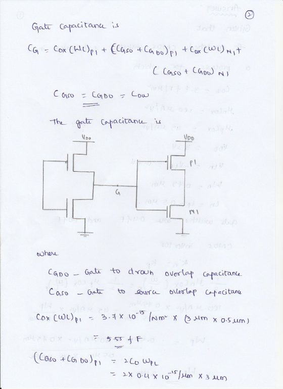
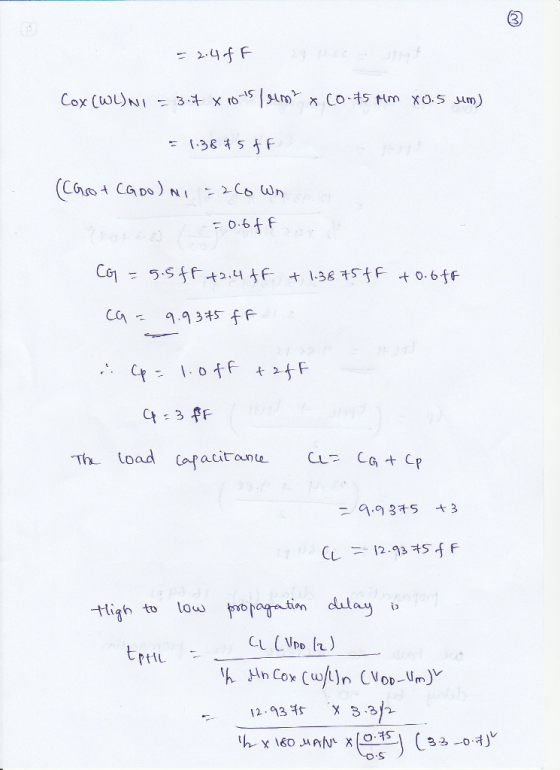
Problem 1 A matched CMOS inverter fabricated in a process for which Cor 3.7 fFjum2, μnCz-180...
For a CMOS inverter fabricated in a 0.18um process with the values given: Value Parameter (W/L)p ...
 For a CMOS inverter fabricated in a 0.18um process with the values given: Value Parameter (W/L)p (W/L)n 1.5 10fF 1.8V Vdd Use the equivalent resistance approach. What is the inverter propagation delay from low to high (tpLH)? Give your answer in pSec, number form to 2 decimal place, no units, no unit prefixes, no commas. Example: 10pS>Answer Given: 10.00
For a CMOS inverter fabricated in a 0.18um process with the values given: Value Parameter (W/L)p (W/L)n 1.5 10fF 1.8V Vdd...
For a CMOS inverter fabricated in a 0.18um process with the values given: Value Parameter (W/L)p (W/L)n 1.5 10fF 1.8V Vdd Use the equivalent resistance approach. What is the inverter propagation delay from low to high (tpLH)? Give your answer in pSec, number form to 2 decimal place, no units, no unit prefixes, no commas. Example: 10pS>Answer Given: 10.00
For a CMOS inverter fabricated in a 0.18um process with the values given: Value Parameter (W/L)p (W/L)n 1.5 10fF 1.8V Vdd...
14.31 Consider a CMOS inverter fabricated in a 65-nm CMOS process for which Vpp = 1V,...
 14.31 Consider a CMOS inverter fabricated in a 65-nm CMOS process for which Vpp = 1V, V = - = 0.35 V, and u C = 2.54 C = 470 HA/V'. In addition, ex and Q, have L = 65 nm and (WIL), = 1.5. (a) Find W that results in V = V 2. What is the silicon area utilized by the inverter in this case? (b) For the matched case in (a), find the values of Vow, VOL...
14.31 Consider a CMOS inverter fabricated in a 65-nm CMOS process for which VopV, V 0.35...
 14.31 Consider a CMOS inverter fabricated in a 65-nm CMOS process for which VopV, V 0.35 v and μη C ,-2.5μ, car-470 μΑ/V2. In addition, QN and QP have L 65 nm and (WIL), = 1.5 (a) Find W, that results in DD/2. What is the silicon area utilized by the inverter in this case? (b) For the matched case in (a), find the values of Vou, Vou» Vi, Vi, NM1, and NMH IH IL' (c) For the matched case...
a. Given a CMOS inverter has gate width Wn-20μm, channel length Lp-La- 2μm, process parameter Kp = 2.0x10⁻⁵A/V2, Kn = 5.0x10⁻⁵A/V2, find the value of (5 marks) the gate width Wp for Bp n b. Given...
 a. Given a CMOS inverter has gate width Wn-20μm, channel length Lp-La- 2μm, process parameter Kp = 2.0x10⁻⁵A/V2, Kn = 5.0x10⁻⁵A/V2, find the value of (5 marks) the gate width Wp for Bp n b. Given that the sheet resistance of the polysilicon is 4.0d the capacitance per unit area of the polysilicon is 0.1fF/um2. Calculate the time constant of a polysilicon polygon with structure shown in the figure, width equals to 3A and the (6 marks) corner resistance is...
A 6T SRAM cell is fabricated in a 0.18 ?m CMOS process for which VDD =...
 A 6T SRAM cell is fabricated in a 0.18 ?m CMOS process for which VDD = 1.8 V, V1-0.5 V, and HmC or 300 ??/V2. The inverters utilize (w/L)n I. Each of the bit lines has a 2 pF capacitance to a. Find the upper bound on WL for each of the access transistors so that Vo and Va do not change by b. Find the delay time ?t encountered in the read operation if the cell design utilizes minimum...
Table 1 Parameters for manual model of 0.13 micron CMOS process DSAT 0.416 0.39 0.297 254 0.14 NM...
 Table 1 Parameters for manual model of 0.13 micron CMOS process DSAT 0.416 0.39 0.297 254 0.14 NMOS PMOS -0.426 -0.29-0583 633 10261 Table 2 Capacitance parameters of NMOS and PMOS transistors in 0.13 micron CMOS process Cox Cov ma MOS 10.7 0.323 0.958 0.395 08 01 0288 0.8 P MOS-110.22ー10.298 11.02ー1042ー08 ー0.107ー0.1ーー0.8 (35 pt Q2 Inverter shown below is implemented in 0.13 um CMOS (8RF). The supply voltage is VDD-1.2 V. Both transistors have a channel length of 0.13...
 For a CMOS inverter fabricated in a 0.18um process with the values given: Value Parameter (W/L)p (W/L)n 1.5 10fF 1.8V Vdd Use the equivalent resistance approach. What is the inverter propagation delay from low to high (tpLH)? Give your answer in pSec, number form to 2 decimal place, no units, no unit prefixes, no commas. Example: 10pS>Answer Given: 10.00
For a CMOS inverter fabricated in a 0.18um process with the values given: Value Parameter (W/L)p (W/L)n 1.5 10fF 1.8V Vdd...
For a CMOS inverter fabricated in a 0.18um process with the values given: Value Parameter (W/L)p (W/L)n 1.5 10fF 1.8V Vdd Use the equivalent resistance approach. What is the inverter propagation delay from low to high (tpLH)? Give your answer in pSec, number form to 2 decimal place, no units, no unit prefixes, no commas. Example: 10pS>Answer Given: 10.00
For a CMOS inverter fabricated in a 0.18um process with the values given: Value Parameter (W/L)p (W/L)n 1.5 10fF 1.8V Vdd...
 14.31 Consider a CMOS inverter fabricated in a 65-nm CMOS process for which Vpp = 1V, V = - = 0.35 V, and u C = 2.54 C = 470 HA/V'. In addition, ex and Q, have L = 65 nm and (WIL), = 1.5. (a) Find W that results in V = V 2. What is the silicon area utilized by the inverter in this case? (b) For the matched case in (a), find the values of Vow, VOL...
 14.31 Consider a CMOS inverter fabricated in a 65-nm CMOS process for which VopV, V 0.35 v and μη C ,-2.5μ, car-470 μΑ/V2. In addition, QN and QP have L 65 nm and (WIL), = 1.5 (a) Find W, that results in DD/2. What is the silicon area utilized by the inverter in this case? (b) For the matched case in (a), find the values of Vou, Vou» Vi, Vi, NM1, and NMH IH IL' (c) For the matched case...
 a. Given a CMOS inverter has gate width Wn-20μm, channel length Lp-La- 2μm, process parameter Kp = 2.0x10⁻⁵A/V2, Kn = 5.0x10⁻⁵A/V2, find the value of (5 marks) the gate width Wp for Bp n b. Given that the sheet resistance of the polysilicon is 4.0d the capacitance per unit area of the polysilicon is 0.1fF/um2. Calculate the time constant of a polysilicon polygon with structure shown in the figure, width equals to 3A and the (6 marks) corner resistance is...
 A 6T SRAM cell is fabricated in a 0.18 ?m CMOS process for which VDD = 1.8 V, V1-0.5 V, and HmC or 300 ??/V2. The inverters utilize (w/L)n I. Each of the bit lines has a 2 pF capacitance to a. Find the upper bound on WL for each of the access transistors so that Vo and Va do not change by b. Find the delay time ?t encountered in the read operation if the cell design utilizes minimum...
 Table 1 Parameters for manual model of 0.13 micron CMOS process DSAT 0.416 0.39 0.297 254 0.14 NMOS PMOS -0.426 -0.29-0583 633 10261 Table 2 Capacitance parameters of NMOS and PMOS transistors in 0.13 micron CMOS process Cox Cov ma MOS 10.7 0.323 0.958 0.395 08 01 0288 0.8 P MOS-110.22ー10.298 11.02ー1042ー08 ー0.107ー0.1ーー0.8 (35 pt Q2 Inverter shown below is implemented in 0.13 um CMOS (8RF). The supply voltage is VDD-1.2 V. Both transistors have a channel length of 0.13...
Most questions answered within 3 hours.
-
Where is the error in this code sequence?
String s1 = "Hello";
String s2 = "ello";...
asked 10 months ago -
Financial data for Joel de Paris, Inc., for last year
follow:
Joel de Paris, Inc.
Balance...
asked 10 months ago -
Consider this reaction:
Al2(SO4)3 (aq)+ BaCl3
(aq) Al2Cl6 (aq)- +
3BaSO4(s) . What is the...
asked 10 months ago -
Suppose that Savneet is considering increasing her
recent random sample from 20 car rentals to 40...
asked 10 months ago -
Trucks arrive at an unloading terminal at an average rate of 120
per hour.
Trucks arrive...
asked 10 months ago -
Why are methanol and ethanol completely soluble in water while
octanol is not very little soluble....
asked 10 months ago -
A facilities manager at a university reads in a research report
that the mean amount of...
asked 10 months ago -
When the CuSO4 is rehydrated by adding water to the anhydrous
compound, is this an endothermic...
asked 10 months ago -
A ray of sunlight is passing from diamond into crown glass; the
angle of incidence is...
asked 10 months ago -
A block of mass 0.249 kg is placed on top of a light, vertical
spring of...
asked 10 months ago -
how do the kidneys compensate in the presences of acidosis
a) trigger hyperventilate
b) reserve acid...
asked 10 months ago -
Question 501 pts
The rental rate of capital to the firm increases. Which of the
following...
asked 10 months ago