
Homework Answers

Add Answer to:
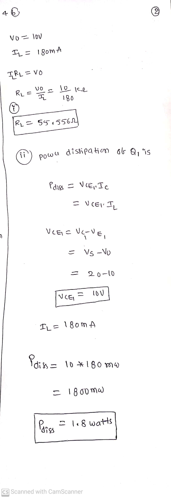
4) a. In the regulator shown in figure 6, R: -60K0, R = 45KN and V2...
*4.57 Consider the voltage-regulator circuit shown in Fig. P4.57. The value of R is selected to...
 *4.57 Consider the voltage-regulator circuit shown in Fig. P4.57. The value of R is selected to obtain an output voltage Vo (across the diode) of 0.7 V. Figure P4.57 (a) Use the diode small-signal model to show that the change in output voltage corresponding to a change of 1 V in Vt is AV AV: = v* +-0.7 V+ V++V, -0.7 This quantity is known as the line regulation and is usually expressed in mV/V. (b) Generalize the expression above...
Q 3. The depletion NMOS amplifier of Figure 2 has R,-50052. RL-10kS2. RSR-RD-5kS2. RG-100kS2. IDD...
 Q 3. The depletion NMOS amplifier of Figure 2 has R,-50052. RL-10kS2. RSR-RD-5kS2. RG-100kS2. IDD 10mA.Vp4V, |VMl 200V, and VDD 12V. Calculate (a) the input resistance Rin /i, (b) the no-load voltage gain Avo-Vo/Vy, (c) the output resistance Ro , and (d) the overall voltage gain A,-uz/vs. RD SR out Figure 2
Q 3. The depletion NMOS amplifier of Figure 2 has R,-50052. RL-10kS2. RSR-RD-5kS2. RG-100kS2. IDD 10mA.Vp4V, |VMl 200V, and VDD 12V. Calculate (a) the input resistance Rin /i,...
Q 3. The depletion NMOS amplifier of Figure 2 has R,-50052. RL-10kS2. RSR-RD-5kS2. RG-100kS2. IDD 10mA.Vp4V, |VMl 200V, and VDD 12V. Calculate (a) the input resistance Rin /i, (b) the no-load voltage gain Avo-Vo/Vy, (c) the output resistance Ro , and (d) the overall voltage gain A,-uz/vs. RD SR out Figure 2
Q 3. The depletion NMOS amplifier of Figure 2 has R,-50052. RL-10kS2. RSR-RD-5kS2. RG-100kS2. IDD 10mA.Vp4V, |VMl 200V, and VDD 12V. Calculate (a) the input resistance Rin /i,...
A three phase full-wave AC controller in Figure Q5(a) is supplied to a system with Y...
 A three phase full-wave AC controller in Figure Q5(a) is supplied to a system with Y connected load system. The load consists of R = 100 and L = 0.01 mH which are connected in series between them. The line-to-line input voltage is given as 208 V with 50 Hz and the delay angle is given as a = 271/3. (1) Calculate the rms value of output phase voltage. (3 marks) (ii) Determine the power factor at output based on...
3. For the regulated power supply shown in Figure 5-3, which is a full-wave bridge rectifier...
 3. For the regulated power supply shown in Figure 5-3, which is a full-wave bridge rectifier containing ter combined with a Zener diode voltage regulator, determine the load voltage VI, load current Ir, source current Is, Zener current Iz and the ripple voltage at the input and output of the regulator, and r(p-p)y respectively, and the ripple frequency fr a fil- VL Ir. Is Iz=. (d-4)1a Ur(p-P) Is V' 1N4002GP Vout = VL + Iz IL 100 V2 120 V...
(c) A loaded zener regulator is shown in Figure 3. Given Vz= 5.1 V at, Iz...
 (c) A loaded zener regulator is shown in Figure 3. Given Vz= 5.1 V at, Iz = 49 mA, Izk= 1 mA, Zz = 72 and Izm= 70 mA. [Satu pengatur beban zener ditunjukkan di dalam Rajah 3. Diberikan V2 = 5.1 V, Iz = 49mA, Izx = 1mA, 2-7 dan Izm = 70mA.] i) Calculate the minimum and the maximum load currents for which the zener diode will maintain the regulation. [Kirakan nilai minima dan maksima arus beban untuk...
Problem 14) : An "enhanced" Voituge Regulator' with a BTT "Current Booster". By crocling to it...
 Problem 14) : An "enhanced" Voituge Regulator' with a BTT "Current Booster". By crocling to it a "power BJT" device as shown, the ordinary Zener ! Voltage regulator can now provide a lood RL a regulated 12.3v DC with a significantly higher DC current 67 0,3A ! The anergizing Source consisting of 18V DC (with mpple Y = 0.5 sin 2407€ votes), is obtained by F.w. rectification and filtering of a portion of the 60-HZ AC Line voltage.. A "V"...
Question 12: [5] The system shown in figure 13 is a basic switching regulator. If the...
 Question 12: [5] The system shown in figure 13 is a basic switching regulator. If the frequency at which the transistor is “switching", is 100Hz with an OFF time of 6 milli seconds, what output voltage is delivered? Also calculate the duty cycle of the transistor. +12 Vo 000 OVOUT } R 4.7k Oscillator fo= 100 Hz (R2 10 k12 For 6 ms R; 15 ΚΩ D2 2.7 V FIGURE 13
Figure 3 Transistor amplifire circuit with source Vs and load R b) For the BJT switching...
 Figure 3 Transistor amplifire circuit with source Vs and load R b) For the BJT switching circuit shown in Figure 4, i) Calculate the value of Ra so that the transistor is operating in saturation when switched on if the value of Rc is 3.9 kn. ii) What will the output voltage be for the applied input signal voltage shown if Vcet IS 0.2V? 5 V Re o V 5 V B 100 OV Figure 4 BUT switching circuit with...
4. Three 100 Sresistors are connected, as shown in Figure 4. The maximum power that can...
 4. Three 100 Sresistors are connected, as shown in Figure 4. The maximum power that can safely be dissipated in any one resistor is 26.5 W. (a) What is the maximum voltage that can be applied to the terminals a and b? (b) For the voltage determined in part (a), what is the power dissipated in each resistor? (c) What is the total power dissipation? 5. A battery has an emf of 15.0 V. The terminal voltage of the battery...
Question 1 In the diagram of Superheterodne AM receiver shown below explain the function of each block. (a) 15 marks Antenna Speaker Audio and power amplifiers RF IF Mixer Detector Mi amplifier a...
 Question 1 In the diagram of Superheterodne AM receiver shown below explain the function of each block. (a) 15 marks Antenna Speaker Audio and power amplifiers RF IF Mixer Detector Mi amplifier amplifier AGC --_Local Gang tuned oscillator (b) For a 4-bit DAC, calculate the output voltage for an input code word 1010 if a [10 marks] logic 1 is 10V and a logic 0 is 0V, and R = RFI kΩ Total: 25 marks] Question 2 (a) Explain the...
 *4.57 Consider the voltage-regulator circuit shown in Fig. P4.57. The value of R is selected to obtain an output voltage Vo (across the diode) of 0.7 V. Figure P4.57 (a) Use the diode small-signal model to show that the change in output voltage corresponding to a change of 1 V in Vt is AV AV: = v* +-0.7 V+ V++V, -0.7 This quantity is known as the line regulation and is usually expressed in mV/V. (b) Generalize the expression above...
 Q 3. The depletion NMOS amplifier of Figure 2 has R,-50052. RL-10kS2. RSR-RD-5kS2. RG-100kS2. IDD 10mA.Vp4V, |VMl 200V, and VDD 12V. Calculate (a) the input resistance Rin /i, (b) the no-load voltage gain Avo-Vo/Vy, (c) the output resistance Ro , and (d) the overall voltage gain A,-uz/vs. RD SR out Figure 2
Q 3. The depletion NMOS amplifier of Figure 2 has R,-50052. RL-10kS2. RSR-RD-5kS2. RG-100kS2. IDD 10mA.Vp4V, |VMl 200V, and VDD 12V. Calculate (a) the input resistance Rin /i,...
Q 3. The depletion NMOS amplifier of Figure 2 has R,-50052. RL-10kS2. RSR-RD-5kS2. RG-100kS2. IDD 10mA.Vp4V, |VMl 200V, and VDD 12V. Calculate (a) the input resistance Rin /i, (b) the no-load voltage gain Avo-Vo/Vy, (c) the output resistance Ro , and (d) the overall voltage gain A,-uz/vs. RD SR out Figure 2
Q 3. The depletion NMOS amplifier of Figure 2 has R,-50052. RL-10kS2. RSR-RD-5kS2. RG-100kS2. IDD 10mA.Vp4V, |VMl 200V, and VDD 12V. Calculate (a) the input resistance Rin /i,...
 A three phase full-wave AC controller in Figure Q5(a) is supplied to a system with Y connected load system. The load consists of R = 100 and L = 0.01 mH which are connected in series between them. The line-to-line input voltage is given as 208 V with 50 Hz and the delay angle is given as a = 271/3. (1) Calculate the rms value of output phase voltage. (3 marks) (ii) Determine the power factor at output based on...
 3. For the regulated power supply shown in Figure 5-3, which is a full-wave bridge rectifier containing ter combined with a Zener diode voltage regulator, determine the load voltage VI, load current Ir, source current Is, Zener current Iz and the ripple voltage at the input and output of the regulator, and r(p-p)y respectively, and the ripple frequency fr a fil- VL Ir. Is Iz=. (d-4)1a Ur(p-P) Is V' 1N4002GP Vout = VL + Iz IL 100 V2 120 V...
 (c) A loaded zener regulator is shown in Figure 3. Given Vz= 5.1 V at, Iz = 49 mA, Izk= 1 mA, Zz = 72 and Izm= 70 mA. [Satu pengatur beban zener ditunjukkan di dalam Rajah 3. Diberikan V2 = 5.1 V, Iz = 49mA, Izx = 1mA, 2-7 dan Izm = 70mA.] i) Calculate the minimum and the maximum load currents for which the zener diode will maintain the regulation. [Kirakan nilai minima dan maksima arus beban untuk...
 Problem 14) : An "enhanced" Voituge Regulator' with a BTT "Current Booster". By crocling to it a "power BJT" device as shown, the ordinary Zener ! Voltage regulator can now provide a lood RL a regulated 12.3v DC with a significantly higher DC current 67 0,3A ! The anergizing Source consisting of 18V DC (with mpple Y = 0.5 sin 2407€ votes), is obtained by F.w. rectification and filtering of a portion of the 60-HZ AC Line voltage.. A "V"...
 Question 12: [5] The system shown in figure 13 is a basic switching regulator. If the frequency at which the transistor is “switching", is 100Hz with an OFF time of 6 milli seconds, what output voltage is delivered? Also calculate the duty cycle of the transistor. +12 Vo 000 OVOUT } R 4.7k Oscillator fo= 100 Hz (R2 10 k12 For 6 ms R; 15 ΚΩ D2 2.7 V FIGURE 13
 Figure 3 Transistor amplifire circuit with source Vs and load R b) For the BJT switching circuit shown in Figure 4, i) Calculate the value of Ra so that the transistor is operating in saturation when switched on if the value of Rc is 3.9 kn. ii) What will the output voltage be for the applied input signal voltage shown if Vcet IS 0.2V? 5 V Re o V 5 V B 100 OV Figure 4 BUT switching circuit with...
 4. Three 100 Sresistors are connected, as shown in Figure 4. The maximum power that can safely be dissipated in any one resistor is 26.5 W. (a) What is the maximum voltage that can be applied to the terminals a and b? (b) For the voltage determined in part (a), what is the power dissipated in each resistor? (c) What is the total power dissipation? 5. A battery has an emf of 15.0 V. The terminal voltage of the battery...
 Question 1 In the diagram of Superheterodne AM receiver shown below explain the function of each block. (a) 15 marks Antenna Speaker Audio and power amplifiers RF IF Mixer Detector Mi amplifier amplifier AGC --_Local Gang tuned oscillator (b) For a 4-bit DAC, calculate the output voltage for an input code word 1010 if a [10 marks] logic 1 is 10V and a logic 0 is 0V, and R = RFI kΩ Total: 25 marks] Question 2 (a) Explain the...
Most questions answered within 3 hours.
-
Where is the error in this code sequence?
String s1 = "Hello";
String s2 = "ello";...
asked 11 months ago -
Financial data for Joel de Paris, Inc., for last year
follow:
Joel de Paris, Inc.
Balance...
asked 11 months ago -
Consider this reaction:
Al2(SO4)3 (aq)+ BaCl3
(aq) Al2Cl6 (aq)- +
3BaSO4(s) . What is the...
asked 11 months ago -
Suppose that Savneet is considering increasing her
recent random sample from 20 car rentals to 40...
asked 11 months ago -
Trucks arrive at an unloading terminal at an average rate of 120
per hour.
Trucks arrive...
asked 11 months ago -
Why are methanol and ethanol completely soluble in water while
octanol is not very little soluble....
asked 11 months ago -
A facilities manager at a university reads in a research report
that the mean amount of...
asked 11 months ago -
When the CuSO4 is rehydrated by adding water to the anhydrous
compound, is this an endothermic...
asked 11 months ago -
A ray of sunlight is passing from diamond into crown glass; the
angle of incidence is...
asked 11 months ago -
A block of mass 0.249 kg is placed on top of a light, vertical
spring of...
asked 11 months ago -
how do the kidneys compensate in the presences of acidosis
a) trigger hyperventilate
b) reserve acid...
asked 11 months ago -
Question 501 pts
The rental rate of capital to the firm increases. Which of the
following...
asked 11 months ago