
Homework Answers
Let a= 10^17 and b= 10^16
Add Answer to:
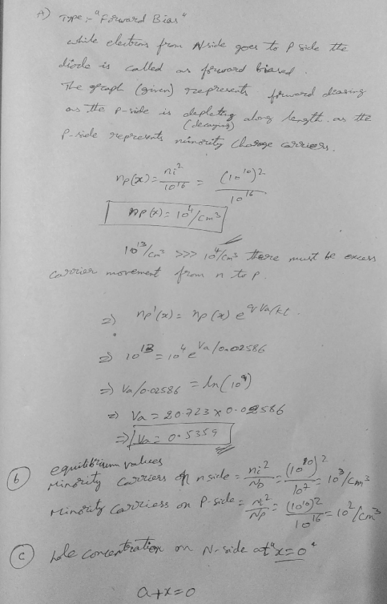
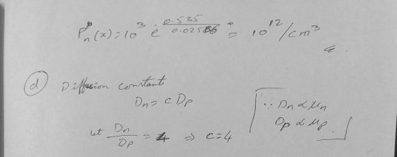
N P n=10 p=109 1013 4.32P) The figure shows carrier densities of a Si PN junction...
this is a problem of semiconductor device and fundamentals. Problem 4: pn Junction Current Distributions Consider a...
 this is a problem of semiconductor device and
fundamentals.
Problem 4: pn Junction Current Distributions Consider a Si pn step junction diode maintained at room temperature, with p-side and n-side dopant concentrations NA 1016 cm3 and Np-2x1016 cm3, respectively. (You may assume that each side is uncompensated.) The minority carrier recombination lifetimes are τ,-10-6 s and τ,-10-7 s on the p-side and n-side, respectively a) Calculate the minority carrier densities at the edges of the depletion region when the applied...
this is a problem of semiconductor device and
fundamentals.
Problem 4: pn Junction Current Distributions Consider a Si pn step junction diode maintained at room temperature, with p-side and n-side dopant concentrations NA 1016 cm3 and Np-2x1016 cm3, respectively. (You may assume that each side is uncompensated.) The minority carrier recombination lifetimes are τ,-10-6 s and τ,-10-7 s on the p-side and n-side, respectively a) Calculate the minority carrier densities at the edges of the depletion region when the applied...
A Si PN junction diode has constant doping at both sides, Na and Nd in P...
A Si PN junction diode has constant doping at both sides, Na and Nd in P and N side, respectively. The width of the P side is W and the width of the N side is L: W << Le and L >> Lh. Le and Lh are the minority carrier diffusion length in each side. The lifetime of both minority carriers is τ. Assume the contacts at both ends of the PN junction are Omic contact. The PN junction...
A pn junction diode is made of a new semiconductor with 10^16cm-3 acceptors in the p...
A pn junction diode is made of a new semiconductor with 10^16cm-3 acceptors in the p side and 2x10^17cm-3 donors on the n-side. Intrinsic carrier concentration is same as silicon 10^10cm-3 at room temperature. Let's assume that a forward bias voltage is applied in a way that it create following minority carrier concentrations in quasi neutral regions. n(x) =10^4 - 10^14/[10^4(x+xp)-1] (cm-3) where x<xp<0 and p(x) = 500+10^15/[10^4(x+xn)+1] (cm-3) where x>xn>0. x is given in cm scale. Calculate the total...
A pn junction diode is made of a new semiconductor with 10^16cm-3 donors in the n...
A pn junction diode is made of a new semiconductor with 10^16cm-3 donors in the n side and 2x10^17cm-3 acceptors on the p-side. Intrinsic carrier concentration is same as silicon 10^10cm-3at room temperature. Let's assume that a forward bias voltage is applied in a way that it create following minority carrier concentrations in quasi neutral regions. p(x) =10^4 + 10^14/[1+10^4(x-xn)] (cm-3) where x>xn>0 and n(x) = 500-10^15/[10^4(x+xp)-1] (cm-3) where x<-xp<0. x is given in cm scale. Calculate the total current...
Design an ideal abrupt silicon PN-junction at 300 K such that the donor impurity concentration in...
 XXX is 467
Design an ideal abrupt silicon PN-junction at 300 K such that the donor impurity concentration in the n-side N, = 5x1015 cm3 and the acceptor impurity concentration in the p-side N, = XXX × 1015/cm3 Assume that the diode area A-2x10⁻³ cm2 and 100cm work Note that the values obtained in the calculations may not be realistic as the Matric # varies greatly. The assignment is only to test your understanding, and must be handwritten Determine the...
XXX is 467
Design an ideal abrupt silicon PN-junction at 300 K such that the donor impurity concentration in the n-side N, = 5x1015 cm3 and the acceptor impurity concentration in the p-side N, = XXX × 1015/cm3 Assume that the diode area A-2x10⁻³ cm2 and 100cm work Note that the values obtained in the calculations may not be realistic as the Matric # varies greatly. The assignment is only to test your understanding, and must be handwritten Determine the...
Ecp 4.20P) The figure shows ban diagram of a Si PN junction diode. Before solution choose...
 Ecp 4.20P) The figure shows ban diagram of a Si PN junction diode. Before solution choose suitable values of a,b and c and show this numbers clearly in a box. a) Calculate the carrier densities plot across the junction (n=1.5 100) b)If you apply reverse bias of 1 V how the carrier densities will change across the junction ?Calculate and plot. Icev Eip- - I a ev Ecn Evp -1 beva EF Ein Eva
E 4.20P) The figure shows ban diagram of a Si PN junction diode. Before solution choose...
 E 4.20P) The figure shows ban diagram of a Si PN junction diode. Before solution choose suitable values of a,b and c and show this numbers clearly in a box. a) Calculate the carrier densities plot across the junction (n=1.5 1019 b)If you apply reverse bias of 1 V how the carrier densities will change across the junction Calculate and plot. ceV Ey- Evp I aev -1 beva En EF En Ev
Problem 3: pn Junction -- Carrier Concentration Profiles The steady-state carrier concentrations inside a Si pn step ju...
 Problem 3: pn Junction -- Carrier Concentration Profiles The steady-state carrier concentrations inside a Si pn step junction diode maintained at room temperature are shown in the plot below: п or p (log scale Pp -106 10 102 a) Is the diode forward or reverse biased? Explain briefly. b) Do low-level injection conditions prevail in the quasi-neutral regions of the diode? Explain briefly. c) What are the p-side and n-side net dopant concentrations NA and ND, respectively? d) Determine the...
Problem 4 (25 points) Consider a silicon pn junction at T-300 K, NA-ND- 1x101° cm3. The minority ...
 Problem 4 (25 points) Consider a silicon pn junction at T-300 K, NA-ND- 1x101° cm3. The minority carrier lifetimes are τ n-0.01 μs and τ p-0.01 us. The junction is forwardbiased with Va 0.6V. The minority carrier diffusion coefficients are Dn-20 cm s, Dp 10 cm Is. n.-1.5x 1010 cm-3 Depletion region n-type p-type a) (10 points) Calculate the excess electron concentration as a function of x in the p side (see the figure above). b) (5 points) Calculate the...
3. An ideal Si pn junction at 300 K is under forward bias. The minority carrier...
 3. An ideal Si pn junction at 300 K is under forward bias. The minority carrier life times are 10* and 107 s for electrons and holes. The doping concentration in the n-region is ND-10° cmPlot the ratio of hole current to the total current crossing the space charge region as the p-region doping concentration (NA varies over the range 1014 to 1018 cnm Use a log scale for the doping concentrations.[use Fig.3.5(a) on P80 for mobility values) 163 cm....
 this is a problem of semiconductor device and
fundamentals.
Problem 4: pn Junction Current Distributions Consider a Si pn step junction diode maintained at room temperature, with p-side and n-side dopant concentrations NA 1016 cm3 and Np-2x1016 cm3, respectively. (You may assume that each side is uncompensated.) The minority carrier recombination lifetimes are τ,-10-6 s and τ,-10-7 s on the p-side and n-side, respectively a) Calculate the minority carrier densities at the edges of the depletion region when the applied...
this is a problem of semiconductor device and
fundamentals.
Problem 4: pn Junction Current Distributions Consider a Si pn step junction diode maintained at room temperature, with p-side and n-side dopant concentrations NA 1016 cm3 and Np-2x1016 cm3, respectively. (You may assume that each side is uncompensated.) The minority carrier recombination lifetimes are τ,-10-6 s and τ,-10-7 s on the p-side and n-side, respectively a) Calculate the minority carrier densities at the edges of the depletion region when the applied...
 XXX is 467
Design an ideal abrupt silicon PN-junction at 300 K such that the donor impurity concentration in the n-side N, = 5x1015 cm3 and the acceptor impurity concentration in the p-side N, = XXX × 1015/cm3 Assume that the diode area A-2x10⁻³ cm2 and 100cm work Note that the values obtained in the calculations may not be realistic as the Matric # varies greatly. The assignment is only to test your understanding, and must be handwritten Determine the...
XXX is 467
Design an ideal abrupt silicon PN-junction at 300 K such that the donor impurity concentration in the n-side N, = 5x1015 cm3 and the acceptor impurity concentration in the p-side N, = XXX × 1015/cm3 Assume that the diode area A-2x10⁻³ cm2 and 100cm work Note that the values obtained in the calculations may not be realistic as the Matric # varies greatly. The assignment is only to test your understanding, and must be handwritten Determine the...
 Ecp 4.20P) The figure shows ban diagram of a Si PN junction diode. Before solution choose suitable values of a,b and c and show this numbers clearly in a box. a) Calculate the carrier densities plot across the junction (n=1.5 100) b)If you apply reverse bias of 1 V how the carrier densities will change across the junction ?Calculate and plot. Icev Eip- - I a ev Ecn Evp -1 beva EF Ein Eva
 E 4.20P) The figure shows ban diagram of a Si PN junction diode. Before solution choose suitable values of a,b and c and show this numbers clearly in a box. a) Calculate the carrier densities plot across the junction (n=1.5 1019 b)If you apply reverse bias of 1 V how the carrier densities will change across the junction Calculate and plot. ceV Ey- Evp I aev -1 beva En EF En Ev
 Problem 3: pn Junction -- Carrier Concentration Profiles The steady-state carrier concentrations inside a Si pn step junction diode maintained at room temperature are shown in the plot below: п or p (log scale Pp -106 10 102 a) Is the diode forward or reverse biased? Explain briefly. b) Do low-level injection conditions prevail in the quasi-neutral regions of the diode? Explain briefly. c) What are the p-side and n-side net dopant concentrations NA and ND, respectively? d) Determine the...
 Problem 4 (25 points) Consider a silicon pn junction at T-300 K, NA-ND- 1x101° cm3. The minority carrier lifetimes are τ n-0.01 μs and τ p-0.01 us. The junction is forwardbiased with Va 0.6V. The minority carrier diffusion coefficients are Dn-20 cm s, Dp 10 cm Is. n.-1.5x 1010 cm-3 Depletion region n-type p-type a) (10 points) Calculate the excess electron concentration as a function of x in the p side (see the figure above). b) (5 points) Calculate the...
 3. An ideal Si pn junction at 300 K is under forward bias. The minority carrier life times are 10* and 107 s for electrons and holes. The doping concentration in the n-region is ND-10° cmPlot the ratio of hole current to the total current crossing the space charge region as the p-region doping concentration (NA varies over the range 1014 to 1018 cnm Use a log scale for the doping concentrations.[use Fig.3.5(a) on P80 for mobility values) 163 cm....
Most questions answered within 3 hours.
-
Where is the error in this code sequence?
String s1 = "Hello";
String s2 = "ello";...
asked 11 months ago -
Financial data for Joel de Paris, Inc., for last year
follow:
Joel de Paris, Inc.
Balance...
asked 11 months ago -
Consider this reaction:
Al2(SO4)3 (aq)+ BaCl3
(aq) Al2Cl6 (aq)- +
3BaSO4(s) . What is the...
asked 11 months ago -
Suppose that Savneet is considering increasing her
recent random sample from 20 car rentals to 40...
asked 11 months ago -
Trucks arrive at an unloading terminal at an average rate of 120
per hour.
Trucks arrive...
asked 11 months ago -
Why are methanol and ethanol completely soluble in water while
octanol is not very little soluble....
asked 11 months ago -
A facilities manager at a university reads in a research report
that the mean amount of...
asked 11 months ago -
When the CuSO4 is rehydrated by adding water to the anhydrous
compound, is this an endothermic...
asked 11 months ago -
A ray of sunlight is passing from diamond into crown glass; the
angle of incidence is...
asked 11 months ago -
A block of mass 0.249 kg is placed on top of a light, vertical
spring of...
asked 11 months ago -
how do the kidneys compensate in the presences of acidosis
a) trigger hyperventilate
b) reserve acid...
asked 11 months ago -
Question 501 pts
The rental rate of capital to the firm increases. Which of the
following...
asked 11 months ago