
Homework Answers

Add Answer to:
Page 6 6. Calculate the following voltages for the circuit below and state the region of...
Solve for the following using: 1) exact method 2) approximate method compare if approximate method is...
 Solve for the following using:
1) exact method
2) approximate method
compare if approximate method is sufficient for analysis. which
solution is better?
Example For the voltage divider bias circuit, RB1-13K2, R 2.2k2 , Rc-68K(2. RE-1.5K(2.Vcc-15 V. VCEsat -0.3 V and β of the Si transistor is 80. Determine the following O" (a) DC base voltage and DC emitter voltage of the transistor amplifier (b) DC operating voltages and currents of the transistor amplifier (lBo, Ico, IEo and VcEO) (c)...
Solve for the following using:
1) exact method
2) approximate method
compare if approximate method is sufficient for analysis. which
solution is better?
Example For the voltage divider bias circuit, RB1-13K2, R 2.2k2 , Rc-68K(2. RE-1.5K(2.Vcc-15 V. VCEsat -0.3 V and β of the Si transistor is 80. Determine the following O" (a) DC base voltage and DC emitter voltage of the transistor amplifier (b) DC operating voltages and currents of the transistor amplifier (lBo, Ico, IEo and VcEO) (c)...
Please explain all steps and reasoning! 6) For the circuit shown below, plot VO and V1...
 Please explain all steps and reasoning!
6) For the circuit shown below, plot VO and V1 as a function of time in the plot shown below. The input voltage on the left is a sawtooth wave show below. The turn on voltage of the diodes are 1 V and 0.7 V as shown below. Use the CVD model Clearly mark the voltages. VNIV OD 0.7V Tapat Villay V San 210 mF Draw your final answer for Vo and V1 in...
Please explain all steps and reasoning!
6) For the circuit shown below, plot VO and V1 as a function of time in the plot shown below. The input voltage on the left is a sawtooth wave show below. The turn on voltage of the diodes are 1 V and 0.7 V as shown below. Use the CVD model Clearly mark the voltages. VNIV OD 0.7V Tapat Villay V San 210 mF Draw your final answer for Vo and V1 in...
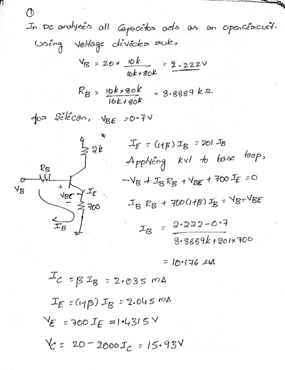
5. Calculate the values for the voltage divider transistor configuration below. Assume 18 = 0 to...
 5. Calculate the values for the voltage divider transistor configuration below. Assume 18 = 0 to solve the circuit. O mA Vc = V8 = Ver VCE = 20 v 38.2 k22 2.7k HE B = 200 1.8k 32.2 k2
In the amplifier circuit below, the transistor has the following properties:Vt =1.5V,k’n=100 microA/V2,W=2 micro m ,L=0.2...
 In the amplifier circuit below, the transistor has the following
properties:Vt =1.5V,k’n=100 microA/V2,W=2 micro m ,L=0.2 micro m,
lambda = 0V^-1
a. Find the dc values VG, VD, and VS.
b. Verify (prove) that the circuit is in the proper region of
operation for an amplifier
c. Find the transconductance value, gm
d. Draw the equivalent small-signal circuit model, replacing the
NMOS with its pi-model
e. Draw the equivalent small-signal circuit model, replacing the
NMOS with its T-model
f. Calculate...
In the amplifier circuit below, the transistor has the following
properties:Vt =1.5V,k’n=100 microA/V2,W=2 micro m ,L=0.2 micro m,
lambda = 0V^-1
a. Find the dc values VG, VD, and VS.
b. Verify (prove) that the circuit is in the proper region of
operation for an amplifier
c. Find the transconductance value, gm
d. Draw the equivalent small-signal circuit model, replacing the
NMOS with its pi-model
e. Draw the equivalent small-signal circuit model, replacing the
NMOS with its T-model
f. Calculate...
Problem 1. Assume the op-amp in the following circuit is ideal. The op-amp supply voltages are:...
 Problem 1. Assume the op-amp in the following circuit is ideal. The op-amp supply voltages are: +V-15V and -Va-15V Use the node voltage method to find the following quantities: a) a b) Va c) Vo (you should get Vo -6.5 V) 50k Ω 30k Ω 10k Ω 10k Ω 0.5 v
Please explain all steps and reasoning! 6) For the circuit shown below, plot VO and V1...
 Please explain all steps and reasoning!
6) For the circuit shown below, plot VO and V1 as a function of time in the plot shown below. The input voltage on the left is a sawtooth wave show below. The turn on voltage of the diodes are 1 V and 0.7 V as shown below. Use the CVD model Clearly mark the voltages. VNIV OD 0.7V Tapat Villay V San 210 mF Draw your final answer for Vo and V1 in...
Please explain all steps and reasoning!
6) For the circuit shown below, plot VO and V1 as a function of time in the plot shown below. The input voltage on the left is a sawtooth wave show below. The turn on voltage of the diodes are 1 V and 0.7 V as shown below. Use the CVD model Clearly mark the voltages. VNIV OD 0.7V Tapat Villay V San 210 mF Draw your final answer for Vo and V1 in...
(2+5 pts) Consider the bias circuit below for a transistor amplifier designed for active region operation....
 (2+5 pts) Consider the bias circuit below for a transistor amplifier designed for active region operation. The desired bias point parameters are lg = 3 mA and Ic = 2.97 mA. Assume VBE- 0.7 V and VT=25 mV. Determine the emitter voltage VE . Choose the best answer. VCC +15 V Vc RBB VB LVE V BB RE 500 S2 1.49 V O2v 01.5V O 0.7V
Consider the NPN transistor circuit below. Assume B=100 and Vee-on=0.7V. Calculate all three DC node voltages...
 Consider the NPN transistor circuit below. Assume B=100 and Vee-on=0.7V. Calculate all three DC node voltages and all five DC branch currents using hand-calculations and then verify in PSPICE using Bias Point Detail Analysis. In PSPICE, use the QBREAKN3 transistor and edit its model with BF=100. Please turn in both your hand-calculation solution and your PSPICE solution including your properly labeled PSPICE schematic. Note that write your hand-calculations right next to the corresponding PSPICE values on your PSPICE printout. Vcc=+15Volts...
Part "c" Please! Consider the circuit below. Assume that the only inductance of interest is the...
 Part "c" Please!
Consider the circuit below. Assume that the only inductance of interest is the load inductor L = 15mH connected to the output terminal. The resistors have the following values: R1 = 5kN, R2 = 2kN, R3 = 0.1kN, and RI, = 10kN. The supply voltage is Vs = 15V. Vs R2 R, vo R1 R3 Figure 6-1 It is known that the input voltage vị can be decomposed into two parts, a constant Vị and a small...
Part "c" Please!
Consider the circuit below. Assume that the only inductance of interest is the load inductor L = 15mH connected to the output terminal. The resistors have the following values: R1 = 5kN, R2 = 2kN, R3 = 0.1kN, and RI, = 10kN. The supply voltage is Vs = 15V. Vs R2 R, vo R1 R3 Figure 6-1 It is known that the input voltage vị can be decomposed into two parts, a constant Vị and a small...
Q #4: (6 marks). For the following circuit, all the transistors are biased in saturation region w...
 Q #4: (6 marks). For the following circuit, all the transistors are biased in saturation region with identical length and width of 1μm and 6.5μm, respectively. It is g 200μΑν-2, Wal Calculate the small signal parameters gm and ro for Q1. What is the value of voltage gain (Av)? iven that, VDD=5V, Vt= 1V, μ.co,- sor and 'REF-0.5mA. Draw the small signal circuit of the following amplifier. VDD es 02 REP ei Vo
Q #4: (6 marks). For the following...
Q #4: (6 marks). For the following circuit, all the transistors are biased in saturation region with identical length and width of 1μm and 6.5μm, respectively. It is g 200μΑν-2, Wal Calculate the small signal parameters gm and ro for Q1. What is the value of voltage gain (Av)? iven that, VDD=5V, Vt= 1V, μ.co,- sor and 'REF-0.5mA. Draw the small signal circuit of the following amplifier. VDD es 02 REP ei Vo
Q #4: (6 marks). For the following...
 Solve for the following using:
1) exact method
2) approximate method
compare if approximate method is sufficient for analysis. which
solution is better?
Example For the voltage divider bias circuit, RB1-13K2, R 2.2k2 , Rc-68K(2. RE-1.5K(2.Vcc-15 V. VCEsat -0.3 V and β of the Si transistor is 80. Determine the following O" (a) DC base voltage and DC emitter voltage of the transistor amplifier (b) DC operating voltages and currents of the transistor amplifier (lBo, Ico, IEo and VcEO) (c)...
Solve for the following using:
1) exact method
2) approximate method
compare if approximate method is sufficient for analysis. which
solution is better?
Example For the voltage divider bias circuit, RB1-13K2, R 2.2k2 , Rc-68K(2. RE-1.5K(2.Vcc-15 V. VCEsat -0.3 V and β of the Si transistor is 80. Determine the following O" (a) DC base voltage and DC emitter voltage of the transistor amplifier (b) DC operating voltages and currents of the transistor amplifier (lBo, Ico, IEo and VcEO) (c)...
 Please explain all steps and reasoning!
6) For the circuit shown below, plot VO and V1 as a function of time in the plot shown below. The input voltage on the left is a sawtooth wave show below. The turn on voltage of the diodes are 1 V and 0.7 V as shown below. Use the CVD model Clearly mark the voltages. VNIV OD 0.7V Tapat Villay V San 210 mF Draw your final answer for Vo and V1 in...
Please explain all steps and reasoning!
6) For the circuit shown below, plot VO and V1 as a function of time in the plot shown below. The input voltage on the left is a sawtooth wave show below. The turn on voltage of the diodes are 1 V and 0.7 V as shown below. Use the CVD model Clearly mark the voltages. VNIV OD 0.7V Tapat Villay V San 210 mF Draw your final answer for Vo and V1 in...
 5. Calculate the values for the voltage divider transistor configuration below. Assume 18 = 0 to solve the circuit. O mA Vc = V8 = Ver VCE = 20 v 38.2 k22 2.7k HE B = 200 1.8k 32.2 k2
 In the amplifier circuit below, the transistor has the following
properties:Vt =1.5V,k’n=100 microA/V2,W=2 micro m ,L=0.2 micro m,
lambda = 0V^-1
a. Find the dc values VG, VD, and VS.
b. Verify (prove) that the circuit is in the proper region of
operation for an amplifier
c. Find the transconductance value, gm
d. Draw the equivalent small-signal circuit model, replacing the
NMOS with its pi-model
e. Draw the equivalent small-signal circuit model, replacing the
NMOS with its T-model
f. Calculate...
In the amplifier circuit below, the transistor has the following
properties:Vt =1.5V,k’n=100 microA/V2,W=2 micro m ,L=0.2 micro m,
lambda = 0V^-1
a. Find the dc values VG, VD, and VS.
b. Verify (prove) that the circuit is in the proper region of
operation for an amplifier
c. Find the transconductance value, gm
d. Draw the equivalent small-signal circuit model, replacing the
NMOS with its pi-model
e. Draw the equivalent small-signal circuit model, replacing the
NMOS with its T-model
f. Calculate...
 Problem 1. Assume the op-amp in the following circuit is ideal. The op-amp supply voltages are: +V-15V and -Va-15V Use the node voltage method to find the following quantities: a) a b) Va c) Vo (you should get Vo -6.5 V) 50k Ω 30k Ω 10k Ω 10k Ω 0.5 v
 Please explain all steps and reasoning!
6) For the circuit shown below, plot VO and V1 as a function of time in the plot shown below. The input voltage on the left is a sawtooth wave show below. The turn on voltage of the diodes are 1 V and 0.7 V as shown below. Use the CVD model Clearly mark the voltages. VNIV OD 0.7V Tapat Villay V San 210 mF Draw your final answer for Vo and V1 in...
Please explain all steps and reasoning!
6) For the circuit shown below, plot VO and V1 as a function of time in the plot shown below. The input voltage on the left is a sawtooth wave show below. The turn on voltage of the diodes are 1 V and 0.7 V as shown below. Use the CVD model Clearly mark the voltages. VNIV OD 0.7V Tapat Villay V San 210 mF Draw your final answer for Vo and V1 in...
 (2+5 pts) Consider the bias circuit below for a transistor amplifier designed for active region operation. The desired bias point parameters are lg = 3 mA and Ic = 2.97 mA. Assume VBE- 0.7 V and VT=25 mV. Determine the emitter voltage VE . Choose the best answer. VCC +15 V Vc RBB VB LVE V BB RE 500 S2 1.49 V O2v 01.5V O 0.7V
 Consider the NPN transistor circuit below. Assume B=100 and Vee-on=0.7V. Calculate all three DC node voltages and all five DC branch currents using hand-calculations and then verify in PSPICE using Bias Point Detail Analysis. In PSPICE, use the QBREAKN3 transistor and edit its model with BF=100. Please turn in both your hand-calculation solution and your PSPICE solution including your properly labeled PSPICE schematic. Note that write your hand-calculations right next to the corresponding PSPICE values on your PSPICE printout. Vcc=+15Volts...
 Part "c" Please!
Consider the circuit below. Assume that the only inductance of interest is the load inductor L = 15mH connected to the output terminal. The resistors have the following values: R1 = 5kN, R2 = 2kN, R3 = 0.1kN, and RI, = 10kN. The supply voltage is Vs = 15V. Vs R2 R, vo R1 R3 Figure 6-1 It is known that the input voltage vị can be decomposed into two parts, a constant Vị and a small...
Part "c" Please!
Consider the circuit below. Assume that the only inductance of interest is the load inductor L = 15mH connected to the output terminal. The resistors have the following values: R1 = 5kN, R2 = 2kN, R3 = 0.1kN, and RI, = 10kN. The supply voltage is Vs = 15V. Vs R2 R, vo R1 R3 Figure 6-1 It is known that the input voltage vị can be decomposed into two parts, a constant Vị and a small...
 Q #4: (6 marks). For the following circuit, all the transistors are biased in saturation region with identical length and width of 1μm and 6.5μm, respectively. It is g 200μΑν-2, Wal Calculate the small signal parameters gm and ro for Q1. What is the value of voltage gain (Av)? iven that, VDD=5V, Vt= 1V, μ.co,- sor and 'REF-0.5mA. Draw the small signal circuit of the following amplifier. VDD es 02 REP ei Vo
Q #4: (6 marks). For the following...
Q #4: (6 marks). For the following circuit, all the transistors are biased in saturation region with identical length and width of 1μm and 6.5μm, respectively. It is g 200μΑν-2, Wal Calculate the small signal parameters gm and ro for Q1. What is the value of voltage gain (Av)? iven that, VDD=5V, Vt= 1V, μ.co,- sor and 'REF-0.5mA. Draw the small signal circuit of the following amplifier. VDD es 02 REP ei Vo
Q #4: (6 marks). For the following...
Most questions answered within 3 hours.
-
Where is the error in this code sequence?
String s1 = "Hello";
String s2 = "ello";...
asked 11 months ago -
Financial data for Joel de Paris, Inc., for last year
follow:
Joel de Paris, Inc.
Balance...
asked 11 months ago -
Consider this reaction:
Al2(SO4)3 (aq)+ BaCl3
(aq) Al2Cl6 (aq)- +
3BaSO4(s) . What is the...
asked 11 months ago -
Suppose that Savneet is considering increasing her
recent random sample from 20 car rentals to 40...
asked 11 months ago -
Trucks arrive at an unloading terminal at an average rate of 120
per hour.
Trucks arrive...
asked 11 months ago -
Why are methanol and ethanol completely soluble in water while
octanol is not very little soluble....
asked 11 months ago -
A facilities manager at a university reads in a research report
that the mean amount of...
asked 11 months ago -
When the CuSO4 is rehydrated by adding water to the anhydrous
compound, is this an endothermic...
asked 11 months ago -
A ray of sunlight is passing from diamond into crown glass; the
angle of incidence is...
asked 11 months ago -
A block of mass 0.249 kg is placed on top of a light, vertical
spring of...
asked 11 months ago -
how do the kidneys compensate in the presences of acidosis
a) trigger hyperventilate
b) reserve acid...
asked 11 months ago -
Question 501 pts
The rental rate of capital to the firm increases. Which of the
following...
asked 11 months ago