
Use the Quartus Prime Text Editor to implement a behavioral model of the D flip-flop described above in a file named d_flops.sv. Specify the D flip-flop’s module according to the interface specification given in the table below.
|
Port |
Mode |
Data Type |
Size |
Description |
|
RST |
in |
logic |
1-bit |
Active high asynchronous reset |
|
CLK |
in |
logic |
1-bit |
Synchronizing clock signal |
|
EN |
in |
logic |
1-bit |
Synchronous clock enable |
|
D |
in |
logic |
1-bit |
Synchronous data input |
|
Q |
out |
logic |
1-bit |
Current/present state |
|
Qbar |
out |
logic |
1-bit |
Inverted current/present state |
Within the module implementation, model the D flip-flop using the following modeling specifications:
-
Declare an intermediate signal named Qtemp of type logic. Signal Qtemprepresents the current state of the D flip-flop.
-
Utilize a concurrent sensitivity-list always_ff @ ( ) statement to represent the behavior of the D flip flop. Which signal(s) should be included in the sensitivity list?(Don’t forget to enclose this in a begin – end block if needed)
-
Within the sensitivity list, detect the rising edge of port signals CLK and RST using the keyword posedge. See the example below:
always_ff @(posedge name_signal)
-
Within the implementation portion of the always @ statement, use nestedsequential if statements to model the behavior of the D flip-flop. What signal(s), if any, have priority? (Don’t forget to enclose this in a begin – end block if needed)
-
Properly assign port signals Q and Qbar.
Homework Answers
//D Flip Flop in SV
module d_flop(
input logic RST,CLK,EN,D, //Input port Declaration
output logic Q,Qbar //Output port Declaration
);
logic Qtemp; //Internal Variable
//Sequential BLOCK using nested if
always_ff @(posedge CLK or posedge RST) begin
if(RST) //Set = 1 or posedge of RST
Qtemp <= 1'b0;
else if(EN) //EN = 1
Qtemp <= D;
else //EN = 0, HOLD previous value
Qtemp <= Qtemp;
end
//Assigning Output Ports
assign Q = Qtemp;
assign Qbar = ~Qtemp;
endmodule
//Testbench in SV
module test;
logic RST,CLK,EN,D,Q,Qbar;
//Instantiation of D Flip Flop
d_flop DFF(RST,CLK,EN,D,Q,Qbar);
//Driving Clock
always begin
#5 CLK = 1'b0;
#5 CLK = ~CLK;
end
//Driving Stimulus
initial begin
RST = 1'b1;
@(posedge CLK) RST = 1'b0;
EN = 0; D = 0;
@(posedge CLK) EN = 0; D = 1;
@(posedge CLK) EN = 1; D = 1;
@(posedge CLK) EN = 1; D = 0;
@(posedge CLK) EN = 1; D = 1;
@(posedge CLK) EN = 0; D = 0;
@(posedge CLK) EN = 1; D = 1;
@(posedge CLK) $finish;s
end
endmodule
//Simulation Waveform

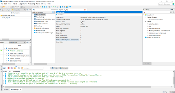
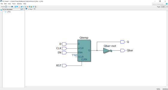
//Quartus Synthesis
Add Answer to:
Use the Quartus Prime Text Editor to implement a behavioral model of the D flip-flop described ab...
Use the Quartus Prime Text Editor to implement a structural model of the 4-bit data register show...
 Use the Quartus Prime Text Editor to implement a structural
model of the 4-bit data register shown above in a file named
reg_4bit.sv. Specify the 4-bit data register’s module according to
the interface specification given in the table below.
Port
Mode
Data Type
Size
Description
RST
in
logic
1-bit
Active high asynchronous reset
CLK
in
logic
1-bit
Synchronizing clock signal
EN
in
logic
1-bit
Synchronous clock enable
D
in
logic vector
4-bits
Synchronous data input
Q
out
logic vector
4-bits...
Use the Quartus Prime Text Editor to implement a structural
model of the 4-bit data register shown above in a file named
reg_4bit.sv. Specify the 4-bit data register’s module according to
the interface specification given in the table below.
Port
Mode
Data Type
Size
Description
RST
in
logic
1-bit
Active high asynchronous reset
CLK
in
logic
1-bit
Synchronizing clock signal
EN
in
logic
1-bit
Synchronous clock enable
D
in
logic vector
4-bits
Synchronous data input
Q
out
logic vector
4-bits...
a) (5 marks) Explain the difference between a latch, a gated latch and a flip flop....
 a) (5 marks) Explain the difference between a latch, a gated latch and a flip flop. b) (5 marks) A gated SR latch has the following schematic diagram CLK a) Draw a timing diagram showing the Q and Q outputs for the following sequence of inputs: CLK R Assume that the initial state of the outputs is Q 0 and Q 1 c) (5 marks) Draw a schematic diagram for a rising edge-triggered master-slave D flip- flop built using two...
3. Answer the following questions about a data flip-flop (D-Flip Flop): a) (4 ps) Write the VHDL required to define a rising-edge triggered (RET) D-Flip Flop with additional clock enable (CEN) an...
 3. Answer the following questions about a data flip-flop (D-Flip Flop): a) (4 ps) Write the VHDL required to define a rising-edge triggered (RET) D-Flip Flop with additional clock enable (CEN) and reset inputs. Your reset may be synchronous or asynchronous. Assume any input, output, or signal variables that you require have already been declared in VHDL (you do not have to write the declarations for these) b) [I pal ls your reset syachronous or asynchronous for the D-Flip Flop...
1. a) Complete the waveform templates for the Master –Slave D-flip-flop below with given D, CLK,...
 1.
a) Complete the waveform templates for the Master –Slave
D-flip-flop below with given D, CLK, CLEAR, and PRESET signals.
Neglect the propagation delays.
b) Does it have positive or negative edge triggering with
respect to CLK?
c) Are the asynchronous PRESET and CLEAR active-high or
active-low?
2. Enabling of data load in the D-flip-flop was implemented with
a 2-to-1 multiplexer as show below. The D-flip-flop has the
positive edge triggering and the active-low asynchronous clear.
a) Is the Enable...
1.
a) Complete the waveform templates for the Master –Slave
D-flip-flop below with given D, CLK, CLEAR, and PRESET signals.
Neglect the propagation delays.
b) Does it have positive or negative edge triggering with
respect to CLK?
c) Are the asynchronous PRESET and CLEAR active-high or
active-low?
2. Enabling of data load in the D-flip-flop was implemented with
a 2-to-1 multiplexer as show below. The D-flip-flop has the
positive edge triggering and the active-low asynchronous clear.
a) Is the Enable...
1. The D Flip-Flop ) Look for the datasheet of the 7474 D flip-flop and wire it on the breadboard...
 1. The D Flip-Flop ) Look for the datasheet of the 7474 D flip-flop and wire it on the breadboard making sure to supply 5V to both Preset and Clear. Utilize the function generator to provide a Clock signal of 1 Hz: i) Press AMPL and set value to 5 Vpp ii) Press FREQ and set value to 1 Hz ili) Press OFFSET and set value to 2.5 V This Clock signal will be the same for all circuits in...
23. A J-K flip-flop has a l on the J input and a 0 on the...
 23. A J-K flip-flop has a l on the J input and a 0 on the K input. What state is the flip-flop in? (a) Q=1,0-0 (b) Q-1, Q-1 (c) Q-0,Q 1 (d) Q-0,Q-0 -24. On a positive edge-triggered S-R flip-flop, the outputs reflect the input condition when (a) the clock pulse is LOW (b) the clock pulse is HIGH (c) the clock pulse transitions from LOW to HIGH (d) the clock pulse transitions from HIGH to LOW 25. The...
I need help doing the code using Verilog modelsim Design a 32-bit register using the D...
I need help doing the code using Verilog modelsim Design a 32-bit register using the D Flip-Flop from part (1) so that it has the following features: (a) The Register has these ports Outputs: Q[31:0] Inputs: D[31:0] CLK is the clock signal EN is a synchronous signal for enabling the register. When EN is asserted at the sensitive edge of the CLK, the input D is loaded into the register. RESET We will leave this input unconnected, but will define...
Consider the circuit in Figure 1. It is a 4-bit (QQ2Q3) synchronous counter which uses four T-typ...
 Consider the circuit in Figure 1. It is a 4-bit (QQ2Q3) synchronous counter which uses four T-type flip-flops. The counter increases its value on each positive edge of the clock if the Enable signal is asserted. The counter is reset to 0 by setting the Clear signal low. You are to implement an 8-bit counter of this type Enable T Q Clock Clear Figure 1. 4-bit synchronous counter (but you need to implement 8-bit counter in this lab) Specific notes:...
We have designed a 2NAND and 3NAND. 1. Use the cells you have already constructed to...
 We have designed a 2NAND and 3NAND.
1. Use the cells you have already constructed to design a latech, and use two latches to build a CMOS D flip-flop schematic in Cadence. Assume the flip-flop is clocked, and that clock, iclock synchronous load and synchronous load are inputs to your design. You must include asynchronous reset signals in your circuit. Load is active iugh. The flip-flop should be positive edge triggered. The clock signal should not be gated (in other...
We have designed a 2NAND and 3NAND.
1. Use the cells you have already constructed to design a latech, and use two latches to build a CMOS D flip-flop schematic in Cadence. Assume the flip-flop is clocked, and that clock, iclock synchronous load and synchronous load are inputs to your design. You must include asynchronous reset signals in your circuit. Load is active iugh. The flip-flop should be positive edge triggered. The clock signal should not be gated (in other...
7. Construct the D-flip-flop with positive-edge triggering and asynchronous Clear (active-low). I...
 7. Construct the D-flip-flop with positive-edge triggering and asynchronous Clear (active-low). Implement the Master-Slave design with two gated D-latches from problem 6 as building blocks and inverters. a) b) Show the schematic. Complete the waveform template below (neglect the propagation delays). Qm and Q are the outputs of the Master and Slave D-latches, respectively. The initial state is unknown. CLK CLK bar CLEAR Qm
7. Construct the D-flip-flop with positive-edge triggering and asynchronous Clear (active-low). Implement the Master-Slave design with...
7. Construct the D-flip-flop with positive-edge triggering and asynchronous Clear (active-low). Implement the Master-Slave design with two gated D-latches from problem 6 as building blocks and inverters. a) b) Show the schematic. Complete the waveform template below (neglect the propagation delays). Qm and Q are the outputs of the Master and Slave D-latches, respectively. The initial state is unknown. CLK CLK bar CLEAR Qm
7. Construct the D-flip-flop with positive-edge triggering and asynchronous Clear (active-low). Implement the Master-Slave design with...
 Use the Quartus Prime Text Editor to implement a structural
model of the 4-bit data register shown above in a file named
reg_4bit.sv. Specify the 4-bit data register’s module according to
the interface specification given in the table below.
Port
Mode
Data Type
Size
Description
RST
in
logic
1-bit
Active high asynchronous reset
CLK
in
logic
1-bit
Synchronizing clock signal
EN
in
logic
1-bit
Synchronous clock enable
D
in
logic vector
4-bits
Synchronous data input
Q
out
logic vector
4-bits...
Use the Quartus Prime Text Editor to implement a structural
model of the 4-bit data register shown above in a file named
reg_4bit.sv. Specify the 4-bit data register’s module according to
the interface specification given in the table below.
Port
Mode
Data Type
Size
Description
RST
in
logic
1-bit
Active high asynchronous reset
CLK
in
logic
1-bit
Synchronizing clock signal
EN
in
logic
1-bit
Synchronous clock enable
D
in
logic vector
4-bits
Synchronous data input
Q
out
logic vector
4-bits...
 a) (5 marks) Explain the difference between a latch, a gated latch and a flip flop. b) (5 marks) A gated SR latch has the following schematic diagram CLK a) Draw a timing diagram showing the Q and Q outputs for the following sequence of inputs: CLK R Assume that the initial state of the outputs is Q 0 and Q 1 c) (5 marks) Draw a schematic diagram for a rising edge-triggered master-slave D flip- flop built using two...
 3. Answer the following questions about a data flip-flop (D-Flip Flop): a) (4 ps) Write the VHDL required to define a rising-edge triggered (RET) D-Flip Flop with additional clock enable (CEN) and reset inputs. Your reset may be synchronous or asynchronous. Assume any input, output, or signal variables that you require have already been declared in VHDL (you do not have to write the declarations for these) b) [I pal ls your reset syachronous or asynchronous for the D-Flip Flop...
 1.
a) Complete the waveform templates for the Master –Slave
D-flip-flop below with given D, CLK, CLEAR, and PRESET signals.
Neglect the propagation delays.
b) Does it have positive or negative edge triggering with
respect to CLK?
c) Are the asynchronous PRESET and CLEAR active-high or
active-low?
2. Enabling of data load in the D-flip-flop was implemented with
a 2-to-1 multiplexer as show below. The D-flip-flop has the
positive edge triggering and the active-low asynchronous clear.
a) Is the Enable...
1.
a) Complete the waveform templates for the Master –Slave
D-flip-flop below with given D, CLK, CLEAR, and PRESET signals.
Neglect the propagation delays.
b) Does it have positive or negative edge triggering with
respect to CLK?
c) Are the asynchronous PRESET and CLEAR active-high or
active-low?
2. Enabling of data load in the D-flip-flop was implemented with
a 2-to-1 multiplexer as show below. The D-flip-flop has the
positive edge triggering and the active-low asynchronous clear.
a) Is the Enable...
 1. The D Flip-Flop ) Look for the datasheet of the 7474 D flip-flop and wire it on the breadboard making sure to supply 5V to both Preset and Clear. Utilize the function generator to provide a Clock signal of 1 Hz: i) Press AMPL and set value to 5 Vpp ii) Press FREQ and set value to 1 Hz ili) Press OFFSET and set value to 2.5 V This Clock signal will be the same for all circuits in...
 23. A J-K flip-flop has a l on the J input and a 0 on the K input. What state is the flip-flop in? (a) Q=1,0-0 (b) Q-1, Q-1 (c) Q-0,Q 1 (d) Q-0,Q-0 -24. On a positive edge-triggered S-R flip-flop, the outputs reflect the input condition when (a) the clock pulse is LOW (b) the clock pulse is HIGH (c) the clock pulse transitions from LOW to HIGH (d) the clock pulse transitions from HIGH to LOW 25. The...
 Consider the circuit in Figure 1. It is a 4-bit (QQ2Q3) synchronous counter which uses four T-type flip-flops. The counter increases its value on each positive edge of the clock if the Enable signal is asserted. The counter is reset to 0 by setting the Clear signal low. You are to implement an 8-bit counter of this type Enable T Q Clock Clear Figure 1. 4-bit synchronous counter (but you need to implement 8-bit counter in this lab) Specific notes:...
 We have designed a 2NAND and 3NAND.
1. Use the cells you have already constructed to design a latech, and use two latches to build a CMOS D flip-flop schematic in Cadence. Assume the flip-flop is clocked, and that clock, iclock synchronous load and synchronous load are inputs to your design. You must include asynchronous reset signals in your circuit. Load is active iugh. The flip-flop should be positive edge triggered. The clock signal should not be gated (in other...
We have designed a 2NAND and 3NAND.
1. Use the cells you have already constructed to design a latech, and use two latches to build a CMOS D flip-flop schematic in Cadence. Assume the flip-flop is clocked, and that clock, iclock synchronous load and synchronous load are inputs to your design. You must include asynchronous reset signals in your circuit. Load is active iugh. The flip-flop should be positive edge triggered. The clock signal should not be gated (in other...
 7. Construct the D-flip-flop with positive-edge triggering and asynchronous Clear (active-low). Implement the Master-Slave design with two gated D-latches from problem 6 as building blocks and inverters. a) b) Show the schematic. Complete the waveform template below (neglect the propagation delays). Qm and Q are the outputs of the Master and Slave D-latches, respectively. The initial state is unknown. CLK CLK bar CLEAR Qm
7. Construct the D-flip-flop with positive-edge triggering and asynchronous Clear (active-low). Implement the Master-Slave design with...
7. Construct the D-flip-flop with positive-edge triggering and asynchronous Clear (active-low). Implement the Master-Slave design with two gated D-latches from problem 6 as building blocks and inverters. a) b) Show the schematic. Complete the waveform template below (neglect the propagation delays). Qm and Q are the outputs of the Master and Slave D-latches, respectively. The initial state is unknown. CLK CLK bar CLEAR Qm
7. Construct the D-flip-flop with positive-edge triggering and asynchronous Clear (active-low). Implement the Master-Slave design with...
Most questions answered within 3 hours.
-
Where is the error in this code sequence?
String s1 = "Hello";
String s2 = "ello";...
asked 11 months ago -
Financial data for Joel de Paris, Inc., for last year
follow:
Joel de Paris, Inc.
Balance...
asked 11 months ago -
Consider this reaction:
Al2(SO4)3 (aq)+ BaCl3
(aq) Al2Cl6 (aq)- +
3BaSO4(s) . What is the...
asked 11 months ago -
Suppose that Savneet is considering increasing her
recent random sample from 20 car rentals to 40...
asked 11 months ago -
Trucks arrive at an unloading terminal at an average rate of 120
per hour.
Trucks arrive...
asked 11 months ago -
Why are methanol and ethanol completely soluble in water while
octanol is not very little soluble....
asked 11 months ago -
A facilities manager at a university reads in a research report
that the mean amount of...
asked 11 months ago -
When the CuSO4 is rehydrated by adding water to the anhydrous
compound, is this an endothermic...
asked 11 months ago -
A ray of sunlight is passing from diamond into crown glass; the
angle of incidence is...
asked 11 months ago -
A block of mass 0.249 kg is placed on top of a light, vertical
spring of...
asked 11 months ago -
how do the kidneys compensate in the presences of acidosis
a) trigger hyperventilate
b) reserve acid...
asked 11 months ago -
Question 501 pts
The rental rate of capital to the firm increases. Which of the
following...
asked 11 months ago