

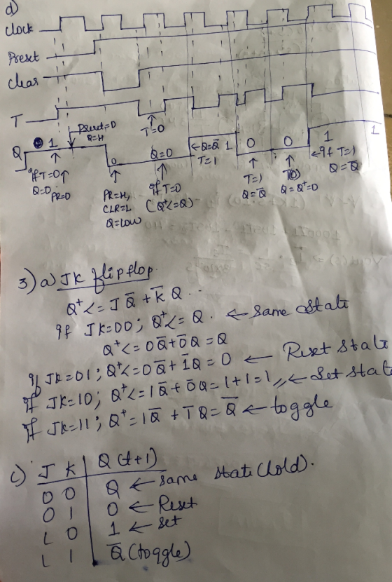
2. The T Flip-Flop a) Build the circuit below equivalent to a T flip-flop. Remember to provide 5V to both Preset and Clear for the D flip-flop. Use a 1 Hz Clock signal. Use resistors and LEDs to monitor the outputs. D a b) How does output Q behave in response to input T? c) With the information gathered from step b), fill out the characteristic table corresponding to a T flip-flop. 0 d) With the information gathered from step c), complete the following timing diagram. Olock Preset
3. The JK Flip-Flop a) Look for the datasheet of the 7476 JK flip-flop and wire it on the breadboard making sure to supply 5V to both Preset and Clear. Use a 1 Hz Clock signal. Use resistors and LEDs to monitor the outputs. The provided JK flip-flop is a negative-edge-triggered device with asynchronous Preset and Clear b) How does output Q behave in response to all four different combinations of inputs Jand K? c) With the information gathered from step b), fill out the characteristic table corresponding to a JK flip-flop. 0 d) e) Change input Clear to LOW and record the outcome. Q f With the information gathered from steps a) through e) above, complete the following timing Change input Preset to Low and record the outcome. Q = Change input Preset back to HIGH. Change input Clear back to HIGH. diagram. Clock Preset Cear
4. The Three-bit Ripple Counter a) Build and demonstrate to the lab instructor the circuit shown below using resistors in series with LEDs to monitor outputs A, B and C. When the input signal Set is LOW every output is also LOW, when the input signal Set is HIGH the circuit becomes operational. vce เงิ NFFF Clock CLPN 10 CLRN CLRN Set b) Observe the behavior of the circuit above and complete the following timing diagram
Homework Answers

Add Answer to:
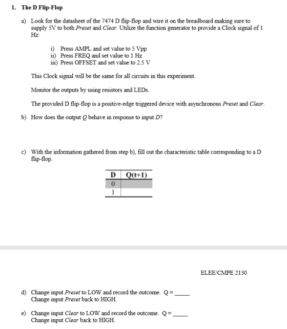
1. The D Flip-Flop ) Look for the datasheet of the 7474 D flip-flop and wire it on the breadboard...
For the input shown below, draw the timing diagrams for the flip flop output Q (assume...
 For the input shown below, draw the timing diagrams for the flip flop output Q (assume negative edge triggered flip flops) 1 CLOCK D or T CLR PRE 1.1 Assume a D flip-flop without a clear or preset 1.2 Assume a D flip-flop with active low clear CLR' 1.3 Assume a D flip-flop with active low clear CLR' and preset PRE 1.4 Assume a T flip-flop without a clear or preset (Q is initially 1) 1.5 Assume a T flip-flop...
UUUUWW PUCH ( WIN) (1) Flip Flop Operation: a. Given the following D Flip Flop circuit...
 UUUUWW PUCH ( WIN) (1) Flip Flop Operation: a. Given the following D Flip Flop circuit and Function Table, complete the timing diagram for Q. Function Table Outputs Inputs CLR XXX III II XXX IX (Note 1) (Note 1) - HE HIGH Logie Level XEther LOW HIGH Logic Level LLOW Loge Level Positive going transition of the clock The output logic level of before the indicated in conditions were established Note: This conti ophen the preset and for clear inputs...
Question 3. [20 marks a) Convert a JK - Flip Flop into a D- Flip Flop...
 Question 3. [20 marks a) Convert a JK - Flip Flop into a D- Flip Flop [10 marks] b) Given the following JK - Flip Flop Preset dCLK K Clear Clearo Preset J K C CLK 1 Figure 2. Timing Diagram Sketch the output waveform Q in Figure 2. [10 marks C
1. a) Complete the waveform templates for the Master –Slave D-flip-flop below with given D, CLK,...
 1.
a) Complete the waveform templates for the Master –Slave
D-flip-flop below with given D, CLK, CLEAR, and PRESET signals.
Neglect the propagation delays.
b) Does it have positive or negative edge triggering with
respect to CLK?
c) Are the asynchronous PRESET and CLEAR active-high or
active-low?
2. Enabling of data load in the D-flip-flop was implemented with
a 2-to-1 multiplexer as show below. The D-flip-flop has the
positive edge triggering and the active-low asynchronous clear.
a) Is the Enable...
1.
a) Complete the waveform templates for the Master –Slave
D-flip-flop below with given D, CLK, CLEAR, and PRESET signals.
Neglect the propagation delays.
b) Does it have positive or negative edge triggering with
respect to CLK?
c) Are the asynchronous PRESET and CLEAR active-high or
active-low?
2. Enabling of data load in the D-flip-flop was implemented with
a 2-to-1 multiplexer as show below. The D-flip-flop has the
positive edge triggering and the active-low asynchronous clear.
a) Is the Enable...
Please give me explanation. The JK flip-flop 1. The figure below is a timing diagram for...
 Please give me
explanation.
The JK flip-flop 1. The figure below is a timing diagram for the J, K, and clock inputs of a positive edge-triggered JK-flip-flop. Draw the corresponding Q and Q' outputs. (4 points) clockoUU Q'
Please give me
explanation.
The JK flip-flop 1. The figure below is a timing diagram for the J, K, and clock inputs of a positive edge-triggered JK-flip-flop. Draw the corresponding Q and Q' outputs. (4 points) clockoUU Q'
4.16 The circuit of Fig. P4.16a contains a JK flip-flop and a D flip-flop. Complete the...
 4.16 The circuit of Fig. P4.16a contains a JK flip-flop and a D flip-flop. Complete the timing diagram of Fig. P4.16b by drawing the waveforms of signals and Q. oc Lep roc Clock bs Clock__ CRU 2 Figure P4.16: a. Logic diagram. B. Timing diagram.
1. Draw the timing diagram for a negative-edge-triggered D flip-flop with Preset and Clear functionalities for...
 1. Draw the timing diagram for a negative-edge-triggered D flip-flop with Preset and Clear functionalities for the following input signal combina- tions. The signal values for Clock, D, Preset, and Clear vary as shown below. Assume each signal is held constant from one-time step to the next. Assume gate delays to be zero. Assume the initial value of Q to be 0. The truth table is shown on the next page. (a) Draw the wave forms for Clock, D, Presetn,...
Use the Quartus Prime Text Editor to implement a behavioral model of the D flip-flop described ab...
 Use the Quartus Prime Text Editor to implement a behavioral
model of the D flip-flop described above in a file named
d_flops.sv. Specify the D flip-flop’s module according to the
interface specification given in the table below.
Port
Mode
Data Type
Size
Description
RST
in
logic
1-bit
Active high asynchronous reset
CLK
in
logic
1-bit
Synchronizing clock signal
EN
in
logic
1-bit
Synchronous clock enable
D
in
logic
1-bit
Synchronous data input
Q
out
logic
1-bit
Current/present state
Qbar
out...
Use the Quartus Prime Text Editor to implement a behavioral
model of the D flip-flop described above in a file named
d_flops.sv. Specify the D flip-flop’s module according to the
interface specification given in the table below.
Port
Mode
Data Type
Size
Description
RST
in
logic
1-bit
Active high asynchronous reset
CLK
in
logic
1-bit
Synchronizing clock signal
EN
in
logic
1-bit
Synchronous clock enable
D
in
logic
1-bit
Synchronous data input
Q
out
logic
1-bit
Current/present state
Qbar
out...
hi i need answers for nos. 18-28. 1. In a counter, a flip-flop output 10. A...
 hi i need answers for nos. 18-28.
1. In a counter, a flip-flop output 10. A is a group of flip-flops, each one of which transition serves as a source for triggering other flip-flops, not by the common clock pulses. shares a common clock and is capable of storing one bit of information. A) RAM B) latch A ripple Cring (rather than signal transitions) are referred to as B synchronous D binary C) counter D) register 11. The Characteristic Equation...
hi i need answers for nos. 18-28.
1. In a counter, a flip-flop output 10. A is a group of flip-flops, each one of which transition serves as a source for triggering other flip-flops, not by the common clock pulses. shares a common clock and is capable of storing one bit of information. A) RAM B) latch A ripple Cring (rather than signal transitions) are referred to as B synchronous D binary C) counter D) register 11. The Characteristic Equation...
23. A J-K flip-flop has a l on the J input and a 0 on the...
 23. A J-K flip-flop has a l on the J input and a 0 on the K input. What state is the flip-flop in? (a) Q=1,0-0 (b) Q-1, Q-1 (c) Q-0,Q 1 (d) Q-0,Q-0 -24. On a positive edge-triggered S-R flip-flop, the outputs reflect the input condition when (a) the clock pulse is LOW (b) the clock pulse is HIGH (c) the clock pulse transitions from LOW to HIGH (d) the clock pulse transitions from HIGH to LOW 25. The...
 For the input shown below, draw the timing diagrams for the flip flop output Q (assume negative edge triggered flip flops) 1 CLOCK D or T CLR PRE 1.1 Assume a D flip-flop without a clear or preset 1.2 Assume a D flip-flop with active low clear CLR' 1.3 Assume a D flip-flop with active low clear CLR' and preset PRE 1.4 Assume a T flip-flop without a clear or preset (Q is initially 1) 1.5 Assume a T flip-flop...
 UUUUWW PUCH ( WIN) (1) Flip Flop Operation: a. Given the following D Flip Flop circuit and Function Table, complete the timing diagram for Q. Function Table Outputs Inputs CLR XXX III II XXX IX (Note 1) (Note 1) - HE HIGH Logie Level XEther LOW HIGH Logic Level LLOW Loge Level Positive going transition of the clock The output logic level of before the indicated in conditions were established Note: This conti ophen the preset and for clear inputs...
 Question 3. [20 marks a) Convert a JK - Flip Flop into a D- Flip Flop [10 marks] b) Given the following JK - Flip Flop Preset dCLK K Clear Clearo Preset J K C CLK 1 Figure 2. Timing Diagram Sketch the output waveform Q in Figure 2. [10 marks C
 1.
a) Complete the waveform templates for the Master –Slave
D-flip-flop below with given D, CLK, CLEAR, and PRESET signals.
Neglect the propagation delays.
b) Does it have positive or negative edge triggering with
respect to CLK?
c) Are the asynchronous PRESET and CLEAR active-high or
active-low?
2. Enabling of data load in the D-flip-flop was implemented with
a 2-to-1 multiplexer as show below. The D-flip-flop has the
positive edge triggering and the active-low asynchronous clear.
a) Is the Enable...
1.
a) Complete the waveform templates for the Master –Slave
D-flip-flop below with given D, CLK, CLEAR, and PRESET signals.
Neglect the propagation delays.
b) Does it have positive or negative edge triggering with
respect to CLK?
c) Are the asynchronous PRESET and CLEAR active-high or
active-low?
2. Enabling of data load in the D-flip-flop was implemented with
a 2-to-1 multiplexer as show below. The D-flip-flop has the
positive edge triggering and the active-low asynchronous clear.
a) Is the Enable...
 Please give me
explanation.
The JK flip-flop 1. The figure below is a timing diagram for the J, K, and clock inputs of a positive edge-triggered JK-flip-flop. Draw the corresponding Q and Q' outputs. (4 points) clockoUU Q'
Please give me
explanation.
The JK flip-flop 1. The figure below is a timing diagram for the J, K, and clock inputs of a positive edge-triggered JK-flip-flop. Draw the corresponding Q and Q' outputs. (4 points) clockoUU Q'
 4.16 The circuit of Fig. P4.16a contains a JK flip-flop and a D flip-flop. Complete the timing diagram of Fig. P4.16b by drawing the waveforms of signals and Q. oc Lep roc Clock bs Clock__ CRU 2 Figure P4.16: a. Logic diagram. B. Timing diagram.
 1. Draw the timing diagram for a negative-edge-triggered D flip-flop with Preset and Clear functionalities for the following input signal combina- tions. The signal values for Clock, D, Preset, and Clear vary as shown below. Assume each signal is held constant from one-time step to the next. Assume gate delays to be zero. Assume the initial value of Q to be 0. The truth table is shown on the next page. (a) Draw the wave forms for Clock, D, Presetn,...
 Use the Quartus Prime Text Editor to implement a behavioral
model of the D flip-flop described above in a file named
d_flops.sv. Specify the D flip-flop’s module according to the
interface specification given in the table below.
Port
Mode
Data Type
Size
Description
RST
in
logic
1-bit
Active high asynchronous reset
CLK
in
logic
1-bit
Synchronizing clock signal
EN
in
logic
1-bit
Synchronous clock enable
D
in
logic
1-bit
Synchronous data input
Q
out
logic
1-bit
Current/present state
Qbar
out...
Use the Quartus Prime Text Editor to implement a behavioral
model of the D flip-flop described above in a file named
d_flops.sv. Specify the D flip-flop’s module according to the
interface specification given in the table below.
Port
Mode
Data Type
Size
Description
RST
in
logic
1-bit
Active high asynchronous reset
CLK
in
logic
1-bit
Synchronizing clock signal
EN
in
logic
1-bit
Synchronous clock enable
D
in
logic
1-bit
Synchronous data input
Q
out
logic
1-bit
Current/present state
Qbar
out...
 hi i need answers for nos. 18-28.
1. In a counter, a flip-flop output 10. A is a group of flip-flops, each one of which transition serves as a source for triggering other flip-flops, not by the common clock pulses. shares a common clock and is capable of storing one bit of information. A) RAM B) latch A ripple Cring (rather than signal transitions) are referred to as B synchronous D binary C) counter D) register 11. The Characteristic Equation...
hi i need answers for nos. 18-28.
1. In a counter, a flip-flop output 10. A is a group of flip-flops, each one of which transition serves as a source for triggering other flip-flops, not by the common clock pulses. shares a common clock and is capable of storing one bit of information. A) RAM B) latch A ripple Cring (rather than signal transitions) are referred to as B synchronous D binary C) counter D) register 11. The Characteristic Equation...
 23. A J-K flip-flop has a l on the J input and a 0 on the K input. What state is the flip-flop in? (a) Q=1,0-0 (b) Q-1, Q-1 (c) Q-0,Q 1 (d) Q-0,Q-0 -24. On a positive edge-triggered S-R flip-flop, the outputs reflect the input condition when (a) the clock pulse is LOW (b) the clock pulse is HIGH (c) the clock pulse transitions from LOW to HIGH (d) the clock pulse transitions from HIGH to LOW 25. The...
Most questions answered within 3 hours.
-
Where is the error in this code sequence?
String s1 = "Hello";
String s2 = "ello";...
asked 11 months ago -
Financial data for Joel de Paris, Inc., for last year
follow:
Joel de Paris, Inc.
Balance...
asked 11 months ago -
Consider this reaction:
Al2(SO4)3 (aq)+ BaCl3
(aq) Al2Cl6 (aq)- +
3BaSO4(s) . What is the...
asked 11 months ago -
Suppose that Savneet is considering increasing her
recent random sample from 20 car rentals to 40...
asked 11 months ago -
Trucks arrive at an unloading terminal at an average rate of 120
per hour.
Trucks arrive...
asked 11 months ago -
Why are methanol and ethanol completely soluble in water while
octanol is not very little soluble....
asked 11 months ago -
A facilities manager at a university reads in a research report
that the mean amount of...
asked 11 months ago -
When the CuSO4 is rehydrated by adding water to the anhydrous
compound, is this an endothermic...
asked 11 months ago -
A ray of sunlight is passing from diamond into crown glass; the
angle of incidence is...
asked 11 months ago -
A block of mass 0.249 kg is placed on top of a light, vertical
spring of...
asked 11 months ago -
how do the kidneys compensate in the presences of acidosis
a) trigger hyperventilate
b) reserve acid...
asked 11 months ago -
Question 501 pts
The rental rate of capital to the firm increases. Which of the
following...
asked 11 months ago