Design a logic circuit (NOR-NOR gates only) , simulate and test the circuit using an Altera Quartus II Software based on the Boolean function below: G1(X, Y, Z) = ∑ m (1,5,6,7) G2 (X, Y, Z) = ∏ M (0,1...
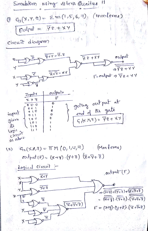
Design a logic circuit (NOR-NOR gates only) , simulate and test the circuit using an Altera Quartus II Software based on the Boolean function below:
G1(X, Y, Z) = ∑ m (1,5,6,7)
G2 (X, Y, Z) = ∏ M (0,1,4,7)
I'm not sure how to design the circuit and how to verify the output using Altera Quartus II, anyone help? Thanks :)
Homework Answers


Add Answer to:
Design a logic circuit (NOR-NOR gates only) , simulate and test the circuit using an Altera Quartus II Software based on the Boolean function below: G1(X, Y, Z) = ∑ m (1,5,6,7) G2 (X, Y, Z) = ∏ M (0,1...
Implement this Boolean Expression on a breadboard using NOR gates Part A: Z =XY+X 'Y' Implement...
 Implement this Boolean Expression on a breadboard using NOR
gates
Part A: Z =XY+X 'Y' Implement this Boolean expression using only NOR gates. Apply De Morgan's law and Boolean laws for the expression to represent it only using NOR operation. Your implementation should use the minimum number of gates (4 NOR gates) required
Implement this Boolean Expression on a breadboard using NOR
gates
Part A: Z =XY+X 'Y' Implement this Boolean expression using only NOR gates. Apply De Morgan's law and Boolean laws for the expression to represent it only using NOR operation. Your implementation should use the minimum number of gates (4 NOR gates) required
Draw a logic diagram using only two-input NOR gates to implement the following function. Show your...
Draw a logic diagram using only two-input NOR gates to implement the following function. Show your work. You must use only NOR gates for this solution, no other gates. You may assume that the inverted inputs are available. Example: if you need A’ as a circuit input, just write A’ as an input name. (15 points) F(A, B, C, D) = (A B)’ (C D) a. Show your work, using Boolean algebra to expand the function to its...
Design a combinational circuit with three inputs, x , y, and z, and three outputs, A,...
Design a combinational circuit with three inputs, x , y, and z, and three outputs, A, B , and C . When the binary input is 0, 1, 2, or 3, the binary output is one greater than the input. When the binary input is 4, 5, 6, or 7, the binary output is two less than the input. 1) Truth table 2) Logic circuit 3) Boolean function of A using minterms ( use Boolean algebra) 4) Boolean function of...
Implement the Boolean function F(w,x,y,z) = Σm(3, 4, 5, 1 1, 12, 13, 14, 15) using a minimum number of NAND gates only.
Implement the Boolean function F(w,x,y,z) = Σm(3, 4, 5, 1 1, 12, 13, 14, 15) using a minimum number of NAND gates only. Write the minimal logic expression (no need to draw the circuit).
We are interested in designing a circuit that implements the following three Boolean functions: 3. h(x,y,z)=Σm(1,4,6)...
 We are interested in designing a circuit that implements the following three Boolean functions: 3. h(x,y,z)=Σm(1,4,6) f1x,y,z)- > m(1,4,6) y-m35) (x,y, z) Σ m (2,4,6,7) 左 You are supposed to implement the circuit with a decoder constructed with NAND gates (a) [12pt] Start by drawing the block diagram of a NAND-based decoder with three inputs (x,y,z), labelling all the outputs with their corresponding Boolean functions (b) [8pt) Using a new block diagram of the NAND-based decoder, implement the circuit using...
Tim Question 1 Atte 20 pts 2H 24 Design a 1-bit Full Adder using NOR gates...
 Tim Question 1 Atte 20 pts 2H 24 Design a 1-bit Full Adder using NOR gates only, you must include and show: Truth tables, detail logic gate circuit designs, and Boolean expressions Upload Choose a File 20 pts Question 2 Design a 4-bit Full Adder with inputs (Xo...X3, Yo...Y3) in which inputs X are connect to two 4-bit registers via four 2-to-1 Multiplexers and inputs Y are connected to two other 4-bit registers via four 2-to-1 Multiplexers. In this case...
Write the Boolean expression that implements the function, F(W,X,Y,Z) = ∑m(1,7,8,10,13) as a 4. NAND-NAND circuit...
Write the Boolean expression that implements the function, F(W,X,Y,Z) = ∑m(1,7,8,10,13) as a 4. NAND-NAND circuit 5. OR-NAND circuit 6. NOR-OR 7. Construct the truth table, K-map minimization, boolean expressions and circuit diagrams for all output bits of a circuit that performs 1’s complement of a 4-bit binary number. Assume overflow bits are lost:
1. (15 pts) Simplify the following Boolean functions using K-maps: a. F(x,y,z) = (1,4,5,6,7) b. F(x,...
 1. (15 pts) Simplify the following Boolean functions using K-maps: a. F(x,y,z) = (1,4,5,6,7) b. F(x, y, z) = (xy + xyz + xyz c. F(A,B,C,D) = 20,2,4,5,6,7,8,10,13,15) d. F(A,B,C,D) = A'B'C'D' + AB'C + B'CD' + ABCD' + BC'D e. F(A,B,C,D,E) = (0,1,4,5,16,17,21,25,29) 2. (12 pts) Consider the combinational logic circuit below and answer the following: a. Derive the Boolean expressions for Fi and F2 as functions of A, B, C, and D. b. List the complete truth table...
Design a PLA that implements the followingthree boolean function A(w,x,y,z) = ?m(4, 5, 7, 12, 13,...
Design a PLA that implements the followingthree boolean function A(w,x,y,z) = ?m(4, 5, 7, 12, 13, 15) B(w,x,y,z) = ?m(0, 1, 4, 5, 8, 9, 11, 12, 13, 15) C(w,x,y,z) = ?m(0, 1, 2, 3, 6, 7, 8, 9, 10, 11, 14) a) Use Karnaugh Maps to optimal each function and its complement. b)Select the three optimal functions to use in the PLA. C)Optimize the equation(s) using Karnaugh Map(s). d.Draw the circuit (Don't forget the clock).
a. Design and implement a combinational circuit with four inputs w,x, y and z and four outputs A, B,C and D using CMOS...
 a. Design and implement a combinational circuit with four inputs w,x, y and z and four outputs A, B,C and D using CMOS transistors. When the binary input is 0, 1, 2,3, 4, 5, 6 or 7 the binary output is three greater than the input. When the binary input is 8,10,11,12,13,14 or 15 the binary output is five less than the input. b. Draw the mask layout with Ln Lp 0.6 um, Wn- 4.8 um and Wp- 9.6 um...
 Implement this Boolean Expression on a breadboard using NOR
gates
Part A: Z =XY+X 'Y' Implement this Boolean expression using only NOR gates. Apply De Morgan's law and Boolean laws for the expression to represent it only using NOR operation. Your implementation should use the minimum number of gates (4 NOR gates) required
Implement this Boolean Expression on a breadboard using NOR
gates
Part A: Z =XY+X 'Y' Implement this Boolean expression using only NOR gates. Apply De Morgan's law and Boolean laws for the expression to represent it only using NOR operation. Your implementation should use the minimum number of gates (4 NOR gates) required
 We are interested in designing a circuit that implements the following three Boolean functions: 3. h(x,y,z)=Σm(1,4,6) f1x,y,z)- > m(1,4,6) y-m35) (x,y, z) Σ m (2,4,6,7) 左 You are supposed to implement the circuit with a decoder constructed with NAND gates (a) [12pt] Start by drawing the block diagram of a NAND-based decoder with three inputs (x,y,z), labelling all the outputs with their corresponding Boolean functions (b) [8pt) Using a new block diagram of the NAND-based decoder, implement the circuit using...
 Tim Question 1 Atte 20 pts 2H 24 Design a 1-bit Full Adder using NOR gates only, you must include and show: Truth tables, detail logic gate circuit designs, and Boolean expressions Upload Choose a File 20 pts Question 2 Design a 4-bit Full Adder with inputs (Xo...X3, Yo...Y3) in which inputs X are connect to two 4-bit registers via four 2-to-1 Multiplexers and inputs Y are connected to two other 4-bit registers via four 2-to-1 Multiplexers. In this case...
 1. (15 pts) Simplify the following Boolean functions using K-maps: a. F(x,y,z) = (1,4,5,6,7) b. F(x, y, z) = (xy + xyz + xyz c. F(A,B,C,D) = 20,2,4,5,6,7,8,10,13,15) d. F(A,B,C,D) = A'B'C'D' + AB'C + B'CD' + ABCD' + BC'D e. F(A,B,C,D,E) = (0,1,4,5,16,17,21,25,29) 2. (12 pts) Consider the combinational logic circuit below and answer the following: a. Derive the Boolean expressions for Fi and F2 as functions of A, B, C, and D. b. List the complete truth table...
 a. Design and implement a combinational circuit with four inputs w,x, y and z and four outputs A, B,C and D using CMOS transistors. When the binary input is 0, 1, 2,3, 4, 5, 6 or 7 the binary output is three greater than the input. When the binary input is 8,10,11,12,13,14 or 15 the binary output is five less than the input. b. Draw the mask layout with Ln Lp 0.6 um, Wn- 4.8 um and Wp- 9.6 um...
Most questions answered within 3 hours.
-
Where is the error in this code sequence?
String s1 = "Hello";
String s2 = "ello";...
asked 10 months ago -
Financial data for Joel de Paris, Inc., for last year
follow:
Joel de Paris, Inc.
Balance...
asked 10 months ago -
Consider this reaction:
Al2(SO4)3 (aq)+ BaCl3
(aq) Al2Cl6 (aq)- +
3BaSO4(s) . What is the...
asked 10 months ago -
Suppose that Savneet is considering increasing her
recent random sample from 20 car rentals to 40...
asked 10 months ago -
Trucks arrive at an unloading terminal at an average rate of 120
per hour.
Trucks arrive...
asked 10 months ago -
Why are methanol and ethanol completely soluble in water while
octanol is not very little soluble....
asked 10 months ago -
A facilities manager at a university reads in a research report
that the mean amount of...
asked 10 months ago -
When the CuSO4 is rehydrated by adding water to the anhydrous
compound, is this an endothermic...
asked 10 months ago -
A ray of sunlight is passing from diamond into crown glass; the
angle of incidence is...
asked 10 months ago -
A block of mass 0.249 kg is placed on top of a light, vertical
spring of...
asked 10 months ago -
how do the kidneys compensate in the presences of acidosis
a) trigger hyperventilate
b) reserve acid...
asked 10 months ago -
Question 501 pts
The rental rate of capital to the firm increases. Which of the
following...
asked 10 months ago