
Homework Answers


Add Answer to:
The layout of a CMOS complex logic circuit is given in the Figure 1. 4. Draw the corresponding circuit diagram; and (10 Marks) a. b. Colculate the W/Doivalent of all the nMOS and PMOS transistors...
The layout of a CMOS complex logic circuit is given in the Figure 1 4. Draw the corresponding circuit diagram; and (10 Marks) a. b. Calculate the (W) of all the nMOS and PMOS transistors for simul...
 The layout of a CMOS complex logic circuit is given in the Figure 1 4. Draw the corresponding circuit diagram; and (10 Marks) a. b. Calculate the (W) of all the nMOS and PMOS transistors for simultaneous switching (W/), 15 for all of all the inputs, assuming that (Wh),-20 for all pMOS transistors and (w/L), = 15 for all (WL 20 for all pMOS transistors and (10 Marks) nMOS transistors VDD n well metal poly silicon n+ diffussion OUT Contact...
with details and explanations 4. The layout of a CMOS complex logic circuit is eiven in the Figure 1 (10 Marks) Calculate the (/equvalent of all the nMoS and PMOS transistors for simultaneous swit...
 with details and explanations
4. The layout of a CMOS complex logic circuit is eiven in the Figure 1 (10 Marks) Calculate the (/equvalent of all the nMoS and PMOS transistors for simultaneous switching of all the inputs, assuming that (W/1), 15 for all pMOS transistors and (W/L), 5 for all nMOS Draw the corresponding circuit diagram; and a. b. (10 Marks) transistors Vdd PMOS NMOS GND Figure 1
4. The layout of a CMOS complex logic circuit is eiven...
with details and explanations
4. The layout of a CMOS complex logic circuit is eiven in the Figure 1 (10 Marks) Calculate the (/equvalent of all the nMoS and PMOS transistors for simultaneous switching of all the inputs, assuming that (W/1), 15 for all pMOS transistors and (W/L), 5 for all nMOS Draw the corresponding circuit diagram; and a. b. (10 Marks) transistors Vdd PMOS NMOS GND Figure 1
4. The layout of a CMOS complex logic circuit is eiven...
Please with details and explanations The layout of a CMOS complex logic circuit is given in the Figure 1. 4. (10 Marks) Draw the corresponding circuit diagram; and cdlculate the (equivaent of all...
 Please with details and explanations
The layout of a CMOS complex logic circuit is given in the Figure 1. 4. (10 Marks) Draw the corresponding circuit diagram; and cdlculate the (equivaent of all the nMOS and PMOS transistors for simultaneous switching of all the inputs, assuming that (W/L)p = 15 for all pMOS transistors and (w/2), a. 5 for all nMOS (10 Marks) transistors Vdd PMOS IL NMOS Figure 1
The layout of a CMOS complex logic circuit is given...
Please with details and explanations
The layout of a CMOS complex logic circuit is given in the Figure 1. 4. (10 Marks) Draw the corresponding circuit diagram; and cdlculate the (equivaent of all the nMOS and PMOS transistors for simultaneous switching of all the inputs, assuming that (W/L)p = 15 for all pMOS transistors and (w/2), a. 5 for all nMOS (10 Marks) transistors Vdd PMOS IL NMOS Figure 1
The layout of a CMOS complex logic circuit is given...
The layout of a CMOS complex logic circuit is given in the Figure 1. 1. Draw the corresponding circuit diagram; and a....
 The layout of a CMOS complex logic circuit is given in the Figure 1. 1. Draw the corresponding circuit diagram; and a. b. Calculate the (W/equivaientfall the nMOS and PMOS transistors for simultaneous equivalent switching of all the inputs, assuming that (W/L), = 25 for all pMOS transistors and W-20 for all nMOS transistors F(A,B,C,D,E ) A B Figure 1
The layout of a CMOS complex logic circuit is given in the Figure 1. 1. Draw the corresponding circuit diagram;...
The layout of a CMOS complex logic circuit is given in the Figure 1. 1. Draw the corresponding circuit diagram; and a. b. Calculate the (W/equivaientfall the nMOS and PMOS transistors for simultaneous equivalent switching of all the inputs, assuming that (W/L), = 25 for all pMOS transistors and W-20 for all nMOS transistors F(A,B,C,D,E ) A B Figure 1
The layout of a CMOS complex logic circuit is given in the Figure 1. 1. Draw the corresponding circuit diagram;...
4. The layout of a CMOS complex logic circuit is given in the Figure t n A to l nd D using (10 Marks) qulatent of all the nmos and PMos transistors for simultaneous switching of for atl noS a. Dra...
 4. The layout of a CMOS complex logic circuit is given in the Figure t n A to l nd D using (10 Marks) qulatent of all the nmos and PMos transistors for simultaneous switching of for atl noS a. Draw the corresponding circuit diagram; and b. Calculate the (WI/n cqutvatent Of l all the inputs, assuming that (/) 15 for all pMOS transistors and (W/)- a viron ne, (10 Marks) transistors and -Vdd rol pMOS NMOS s GND
4....
4. The layout of a CMOS complex logic circuit is given in the Figure t n A to l nd D using (10 Marks) qulatent of all the nmos and PMos transistors for simultaneous switching of for atl noS a. Draw the corresponding circuit diagram; and b. Calculate the (WI/n cqutvatent Of l all the inputs, assuming that (/) 15 for all pMOS transistors and (W/)- a viron ne, (10 Marks) transistors and -Vdd rol pMOS NMOS s GND
4....
The layout of a CMOS complex logiccircuit is given in the Figure 1 4. (10 Marks) a. Draw the corresponding circuit diagram;and b. calculate the (uivains f allthe nMoS and PMOS transistors for simulta...
 The layout of a CMOS complex logiccircuit is given in the Figure 1 4. (10 Marks) a. Draw the corresponding circuit diagram;and b. calculate the (uivains f allthe nMoS and PMOS transistors for simultaneous switching of all the inputs, assumingthat(W/15 for all pMOS transistors and 10 for all equivalent 15 for all pMOS transistors and(W/D)10for all (10 Marks) nMOS transistors. n+ diffusion p+ diffusion ■ metal OUT polysilicon GND Figure 1
The layout of a CMOS complex logiccircuit is given...
The layout of a CMOS complex logiccircuit is given in the Figure 1 4. (10 Marks) a. Draw the corresponding circuit diagram;and b. calculate the (uivains f allthe nMoS and PMOS transistors for simultaneous switching of all the inputs, assumingthat(W/15 for all pMOS transistors and 10 for all equivalent 15 for all pMOS transistors and(W/D)10for all (10 Marks) nMOS transistors. n+ diffusion p+ diffusion ■ metal OUT polysilicon GND Figure 1
The layout of a CMOS complex logiccircuit is given...
The layout of a CMOS complex logic circuit is given in the Figure 1. Draw the corresponding circuit diagram; and Calcula...
 The layout of a CMOS complex logic circuit is given in the
Figure 1. Draw the corresponding circuit diagram; and
Calculate the (W⁄L)_equivalent of all the nMOS and PMOS
transistors for simultaneous switching of all the inputs, assuming
that (W⁄L)p =20 for all pMOS transistors and (W⁄L)n =15 for all
nMOS transistors.
Windows VDD poly silicon n+ diffussion OUT P+ diffusion Centact GND
Windows VDD poly silicon n+ diffussion OUT P+ diffusion Centact GND
The layout of a CMOS complex logic circuit is given in the
Figure 1. Draw the corresponding circuit diagram; and
Calculate the (W⁄L)_equivalent of all the nMOS and PMOS
transistors for simultaneous switching of all the inputs, assuming
that (W⁄L)p =20 for all pMOS transistors and (W⁄L)n =15 for all
nMOS transistors.
Windows VDD poly silicon n+ diffussion OUT P+ diffusion Centact GND
Windows VDD poly silicon n+ diffussion OUT P+ diffusion Centact GND
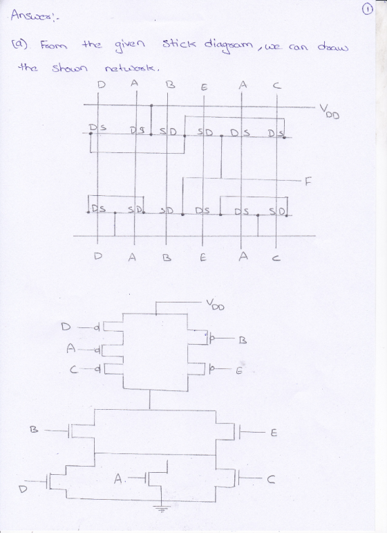
with details and explanations 3. Consider the logic function Z-((A + B).D). (C.(E+F)) (5 Marks) Realize the above Boolean function using CMOS transistors. a. btain a common Euler path for both nMO...
 with details and explanations
3. Consider the logic function Z-((A + B).D). (C.(E+F)) (5 Marks) Realize the above Boolean function using CMOS transistors. a. btain a common Euler path for both nMOS and pMOS transistors and hence draw the optimized stick diagram layout. b. O (30 Marks)
3. Consider the logic function Z-((A + B).D). (C.(E+F)) (5 Marks) Realize the above Boolean function using CMOS transistors. a. btain a common Euler path for both nMOS and pMOS transistors and hence...
with details and explanations
3. Consider the logic function Z-((A + B).D). (C.(E+F)) (5 Marks) Realize the above Boolean function using CMOS transistors. a. btain a common Euler path for both nMOS and pMOS transistors and hence draw the optimized stick diagram layout. b. O (30 Marks)
3. Consider the logic function Z-((A + B).D). (C.(E+F)) (5 Marks) Realize the above Boolean function using CMOS transistors. a. btain a common Euler path for both nMOS and pMOS transistors and hence...
Consider the logic function Zr((A+B). D. (CKE+F))) 3. Realize the sbove Boolean function using CMos transtors. b. Obtain a common Euler path for both DMOS and pMOS transistors and hence draw the opti...
 Consider the logic function Zr((A+B). D. (CKE+F))) 3. Realize the sbove Boolean function using CMos transtors. b. Obtain a common Euler path for both DMOS and pMOS transistors and hence draw the optimized stick diagram layout.
Consider the logic function Zr((A+B). D. (CKE+F))) 3. Realize the sbove Boolean function using CMos transtors. b. Obtain a common Euler path for both DMOS and pMOS transistors and hence draw the optimized stick diagram layout.
Consider the logic function Zr((A+B). D. (CKE+F))) 3. Realize the sbove Boolean function using CMos transtors. b. Obtain a common Euler path for both DMOS and pMOS transistors and hence draw the optimized stick diagram layout.
Prob 2. Implement the logic function Y = (Ā + B)D in static CMOS. a) Size the transistors so that the output resistance is the same as that of a an nMOS (W/L-0.4/0.18) and pMOS (W/L-0.8/0.18). b)...
 Prob 2. Implement the logic function Y = (Ā + B)D in static CMOS. a) Size the transistors so that the output resistance is the same as that of a an nMOS (W/L-0.4/0.18) and pMOS (W/L-0.8/0.18). b) What input combination(s) result in the worst case tpiti.? c) Determine the worst case tpl for a 100 iF load capacitance. Use equivalent resistance model, Req
Prob 2. Implement the logic function Y = (Ā + B)D in static CMOS. a) Size the...
Prob 2. Implement the logic function Y = (Ā + B)D in static CMOS. a) Size the transistors so that the output resistance is the same as that of a an nMOS (W/L-0.4/0.18) and pMOS (W/L-0.8/0.18). b) What input combination(s) result in the worst case tpiti.? c) Determine the worst case tpl for a 100 iF load capacitance. Use equivalent resistance model, Req
Prob 2. Implement the logic function Y = (Ā + B)D in static CMOS. a) Size the...
 The layout of a CMOS complex logic circuit is given in the Figure 1 4. Draw the corresponding circuit diagram; and (10 Marks) a. b. Calculate the (W) of all the nMOS and PMOS transistors for simultaneous switching (W/), 15 for all of all the inputs, assuming that (Wh),-20 for all pMOS transistors and (w/L), = 15 for all (WL 20 for all pMOS transistors and (10 Marks) nMOS transistors VDD n well metal poly silicon n+ diffussion OUT Contact...
 with details and explanations
4. The layout of a CMOS complex logic circuit is eiven in the Figure 1 (10 Marks) Calculate the (/equvalent of all the nMoS and PMOS transistors for simultaneous switching of all the inputs, assuming that (W/1), 15 for all pMOS transistors and (W/L), 5 for all nMOS Draw the corresponding circuit diagram; and a. b. (10 Marks) transistors Vdd PMOS NMOS GND Figure 1
4. The layout of a CMOS complex logic circuit is eiven...
with details and explanations
4. The layout of a CMOS complex logic circuit is eiven in the Figure 1 (10 Marks) Calculate the (/equvalent of all the nMoS and PMOS transistors for simultaneous switching of all the inputs, assuming that (W/1), 15 for all pMOS transistors and (W/L), 5 for all nMOS Draw the corresponding circuit diagram; and a. b. (10 Marks) transistors Vdd PMOS NMOS GND Figure 1
4. The layout of a CMOS complex logic circuit is eiven...
 Please with details and explanations
The layout of a CMOS complex logic circuit is given in the Figure 1. 4. (10 Marks) Draw the corresponding circuit diagram; and cdlculate the (equivaent of all the nMOS and PMOS transistors for simultaneous switching of all the inputs, assuming that (W/L)p = 15 for all pMOS transistors and (w/2), a. 5 for all nMOS (10 Marks) transistors Vdd PMOS IL NMOS Figure 1
The layout of a CMOS complex logic circuit is given...
Please with details and explanations
The layout of a CMOS complex logic circuit is given in the Figure 1. 4. (10 Marks) Draw the corresponding circuit diagram; and cdlculate the (equivaent of all the nMOS and PMOS transistors for simultaneous switching of all the inputs, assuming that (W/L)p = 15 for all pMOS transistors and (w/2), a. 5 for all nMOS (10 Marks) transistors Vdd PMOS IL NMOS Figure 1
The layout of a CMOS complex logic circuit is given...
 The layout of a CMOS complex logic circuit is given in the Figure 1. 1. Draw the corresponding circuit diagram; and a. b. Calculate the (W/equivaientfall the nMOS and PMOS transistors for simultaneous equivalent switching of all the inputs, assuming that (W/L), = 25 for all pMOS transistors and W-20 for all nMOS transistors F(A,B,C,D,E ) A B Figure 1
The layout of a CMOS complex logic circuit is given in the Figure 1. 1. Draw the corresponding circuit diagram;...
The layout of a CMOS complex logic circuit is given in the Figure 1. 1. Draw the corresponding circuit diagram; and a. b. Calculate the (W/equivaientfall the nMOS and PMOS transistors for simultaneous equivalent switching of all the inputs, assuming that (W/L), = 25 for all pMOS transistors and W-20 for all nMOS transistors F(A,B,C,D,E ) A B Figure 1
The layout of a CMOS complex logic circuit is given in the Figure 1. 1. Draw the corresponding circuit diagram;...
 4. The layout of a CMOS complex logic circuit is given in the Figure t n A to l nd D using (10 Marks) qulatent of all the nmos and PMos transistors for simultaneous switching of for atl noS a. Draw the corresponding circuit diagram; and b. Calculate the (WI/n cqutvatent Of l all the inputs, assuming that (/) 15 for all pMOS transistors and (W/)- a viron ne, (10 Marks) transistors and -Vdd rol pMOS NMOS s GND
4....
4. The layout of a CMOS complex logic circuit is given in the Figure t n A to l nd D using (10 Marks) qulatent of all the nmos and PMos transistors for simultaneous switching of for atl noS a. Draw the corresponding circuit diagram; and b. Calculate the (WI/n cqutvatent Of l all the inputs, assuming that (/) 15 for all pMOS transistors and (W/)- a viron ne, (10 Marks) transistors and -Vdd rol pMOS NMOS s GND
4....
 The layout of a CMOS complex logiccircuit is given in the Figure 1 4. (10 Marks) a. Draw the corresponding circuit diagram;and b. calculate the (uivains f allthe nMoS and PMOS transistors for simultaneous switching of all the inputs, assumingthat(W/15 for all pMOS transistors and 10 for all equivalent 15 for all pMOS transistors and(W/D)10for all (10 Marks) nMOS transistors. n+ diffusion p+ diffusion ■ metal OUT polysilicon GND Figure 1
The layout of a CMOS complex logiccircuit is given...
The layout of a CMOS complex logiccircuit is given in the Figure 1 4. (10 Marks) a. Draw the corresponding circuit diagram;and b. calculate the (uivains f allthe nMoS and PMOS transistors for simultaneous switching of all the inputs, assumingthat(W/15 for all pMOS transistors and 10 for all equivalent 15 for all pMOS transistors and(W/D)10for all (10 Marks) nMOS transistors. n+ diffusion p+ diffusion ■ metal OUT polysilicon GND Figure 1
The layout of a CMOS complex logiccircuit is given...
 The layout of a CMOS complex logic circuit is given in the
Figure 1. Draw the corresponding circuit diagram; and
Calculate the (W⁄L)_equivalent of all the nMOS and PMOS
transistors for simultaneous switching of all the inputs, assuming
that (W⁄L)p =20 for all pMOS transistors and (W⁄L)n =15 for all
nMOS transistors.
Windows VDD poly silicon n+ diffussion OUT P+ diffusion Centact GND
Windows VDD poly silicon n+ diffussion OUT P+ diffusion Centact GND
The layout of a CMOS complex logic circuit is given in the
Figure 1. Draw the corresponding circuit diagram; and
Calculate the (W⁄L)_equivalent of all the nMOS and PMOS
transistors for simultaneous switching of all the inputs, assuming
that (W⁄L)p =20 for all pMOS transistors and (W⁄L)n =15 for all
nMOS transistors.
Windows VDD poly silicon n+ diffussion OUT P+ diffusion Centact GND
Windows VDD poly silicon n+ diffussion OUT P+ diffusion Centact GND
 with details and explanations
3. Consider the logic function Z-((A + B).D). (C.(E+F)) (5 Marks) Realize the above Boolean function using CMOS transistors. a. btain a common Euler path for both nMOS and pMOS transistors and hence draw the optimized stick diagram layout. b. O (30 Marks)
3. Consider the logic function Z-((A + B).D). (C.(E+F)) (5 Marks) Realize the above Boolean function using CMOS transistors. a. btain a common Euler path for both nMOS and pMOS transistors and hence...
with details and explanations
3. Consider the logic function Z-((A + B).D). (C.(E+F)) (5 Marks) Realize the above Boolean function using CMOS transistors. a. btain a common Euler path for both nMOS and pMOS transistors and hence draw the optimized stick diagram layout. b. O (30 Marks)
3. Consider the logic function Z-((A + B).D). (C.(E+F)) (5 Marks) Realize the above Boolean function using CMOS transistors. a. btain a common Euler path for both nMOS and pMOS transistors and hence...
 Consider the logic function Zr((A+B). D. (CKE+F))) 3. Realize the sbove Boolean function using CMos transtors. b. Obtain a common Euler path for both DMOS and pMOS transistors and hence draw the optimized stick diagram layout.
Consider the logic function Zr((A+B). D. (CKE+F))) 3. Realize the sbove Boolean function using CMos transtors. b. Obtain a common Euler path for both DMOS and pMOS transistors and hence draw the optimized stick diagram layout.
Consider the logic function Zr((A+B). D. (CKE+F))) 3. Realize the sbove Boolean function using CMos transtors. b. Obtain a common Euler path for both DMOS and pMOS transistors and hence draw the optimized stick diagram layout.
 Prob 2. Implement the logic function Y = (Ā + B)D in static CMOS. a) Size the transistors so that the output resistance is the same as that of a an nMOS (W/L-0.4/0.18) and pMOS (W/L-0.8/0.18). b) What input combination(s) result in the worst case tpiti.? c) Determine the worst case tpl for a 100 iF load capacitance. Use equivalent resistance model, Req
Prob 2. Implement the logic function Y = (Ā + B)D in static CMOS. a) Size the...
Prob 2. Implement the logic function Y = (Ā + B)D in static CMOS. a) Size the transistors so that the output resistance is the same as that of a an nMOS (W/L-0.4/0.18) and pMOS (W/L-0.8/0.18). b) What input combination(s) result in the worst case tpiti.? c) Determine the worst case tpl for a 100 iF load capacitance. Use equivalent resistance model, Req
Prob 2. Implement the logic function Y = (Ā + B)D in static CMOS. a) Size the...
Most questions answered within 3 hours.
-
Where is the error in this code sequence?
String s1 = "Hello";
String s2 = "ello";...
asked 10 months ago -
Financial data for Joel de Paris, Inc., for last year
follow:
Joel de Paris, Inc.
Balance...
asked 10 months ago -
Consider this reaction:
Al2(SO4)3 (aq)+ BaCl3
(aq) Al2Cl6 (aq)- +
3BaSO4(s) . What is the...
asked 10 months ago -
Suppose that Savneet is considering increasing her
recent random sample from 20 car rentals to 40...
asked 10 months ago -
Trucks arrive at an unloading terminal at an average rate of 120
per hour.
Trucks arrive...
asked 10 months ago -
Why are methanol and ethanol completely soluble in water while
octanol is not very little soluble....
asked 10 months ago -
A facilities manager at a university reads in a research report
that the mean amount of...
asked 10 months ago -
When the CuSO4 is rehydrated by adding water to the anhydrous
compound, is this an endothermic...
asked 10 months ago -
A ray of sunlight is passing from diamond into crown glass; the
angle of incidence is...
asked 10 months ago -
A block of mass 0.249 kg is placed on top of a light, vertical
spring of...
asked 10 months ago -
how do the kidneys compensate in the presences of acidosis
a) trigger hyperventilate
b) reserve acid...
asked 10 months ago -
Question 501 pts
The rental rate of capital to the firm increases. Which of the
following...
asked 10 months ago