Assume that ‘slt $1, $2, $3’ is executed with the implementation
in the picture. Identify the value of the 9-bit control
signals.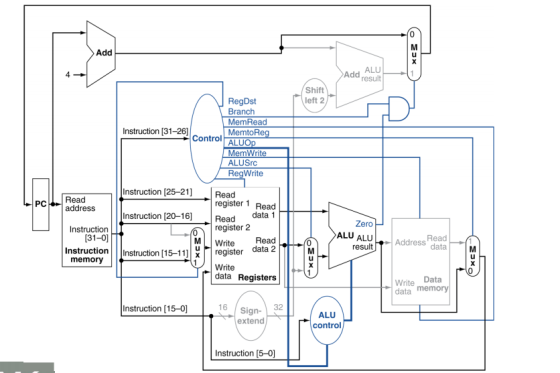
Homework Answers
instruction : slt $1 S2 $3
control signal
RegDst = 1
RegWrite = 1
ALUSrc = 0
ALUOp = 111
MemWrite = 0
MemRead = 0
MemToReg = 0
Add Answer to:
Assume that ‘slt $1, $2, $3’ is executed with the implementation in the picture. Identify the value of the 9-bit control...
*For a clearer view of the datapath* Answer choices for all Consider the MIPS single cycle...
 *For a clearer view of the datapath*
Answer choices for all
Consider the MIPS single cycle datapath shown below. Select the correct control signals that will be generated by the control unit for the following instruction: andi $t0,$t1,4 Instruction (25-01 Shin Jump address (31-0) - left 2) 28 PC +4 [31-28) XCS result left 2 RegDst Jump Branch MemRead Instruction (31-26] MemtoReg Control ALUOP MemWrite ALUSrc RegWrite Instruction (25-21] PC Read address Read register 1 Read Instruction (20-16] Read data...
*For a clearer view of the datapath*
Answer choices for all
Consider the MIPS single cycle datapath shown below. Select the correct control signals that will be generated by the control unit for the following instruction: andi $t0,$t1,4 Instruction (25-01 Shin Jump address (31-0) - left 2) 28 PC +4 [31-28) XCS result left 2 RegDst Jump Branch MemRead Instruction (31-26] MemtoReg Control ALUOP MemWrite ALUSrc RegWrite Instruction (25-21] PC Read address Read register 1 Read Instruction (20-16] Read data...
Q4: Answer the following questions. [7 Marks] The single cycle implementation of MIPS is as shown...
 Q4: Answer the following questions. [7 Marks] The single cycle implementation of MIPS is as shown below. Answer the following questions with reference to "beq $S1, $S2, 8H” instruction. Assume that the contents of the registers S1 = 10 H, S2 = 10H, and PC = 16H, pointing to the instruction under consideration. 1. What is the addressing mode of the instruction? [1] ii. Which part of the instruction format, address of S1 and S2 are stored? [1] 111. What...
(o x Add Addresult ALU Shift left 2 Regst Branch MemRead Instruction (31-26) MemtoReg Controll ALUOP...
 (o x Add Addresult ALU Shift left 2 Regst Branch MemRead Instruction (31-26) MemtoReg Controll ALUOP MemWrite ALUSC RogWrite Instruction [25-21] Read register 1 Read Instruction (20-16) Read data 1 register 2 Write Read Instruction (15-11) Write data Registers PC Read address Zoro ALU ALU Instruction (31-0) Instruction memory result Address Read data register data 2 **039 -25 Write Data data memory Instruction (15-01 16 Sign- extend ALU control Instruction 15-01 With regards to the single cycle implementation (as shown...
A block diagram of MIPS architecture is given below. What is the value of the control...
 A block diagram of MIPS architecture is given below. What is the
value of the control bit for each MUX during the execution of the
given instruction? Note, you may use N/A if MUX output is not
useful.
Add MUX 4 ALU Addresult Shift left 2 RegDst Branch MemRead Instruction (31-26] MemtoReg Control ALUOp MemWrite ALUSrc RegWrite Instruction [25-21] PC Read address Read register 1 Read Read data 1 register 2 Write Read MUX 2 Zero Instruction (2016) MUX(1 Instruction...
A block diagram of MIPS architecture is given below. What is the
value of the control bit for each MUX during the execution of the
given instruction? Note, you may use N/A if MUX output is not
useful.
Add MUX 4 ALU Addresult Shift left 2 RegDst Branch MemRead Instruction (31-26] MemtoReg Control ALUOp MemWrite ALUSrc RegWrite Instruction [25-21] PC Read address Read register 1 Read Read data 1 register 2 Write Read MUX 2 Zero Instruction (2016) MUX(1 Instruction...
MCS) Add Addresult ALU Shift left 2 RegDst Branch MemRead MemtoReg Instruction (31-26] Control ALUOP MemWrite...
 MCS) Add Addresult ALU Shift left 2 RegDst Branch MemRead MemtoReg Instruction (31-26] Control ALUOP MemWrite ALUS RegWrite PC instruction (25-21] Instruction (20-16) Read address Instruction (31-0) Instruction memory Read register 1 Read Read data 1 register 2 Write Read Zoro ALU ALU result Address Read data instruction (15-11] register data 2 x3) Write data Registers Write Data data memory Instruction 15-01 16 Sign- extend ALU control Instruction (5-0) With regards to the single cycle implementation (as shown in the...
it is the same question A block diagram of MIPS architecture is given below. What is...
 it is the same question
A block diagram of MIPS architecture is given below. What is the value of the control bit for each MUX during the execution of the given instruction? Note, you may use N/Aif MUX output is not usefu Add MUX 4 ALU Add, result Shift left 2 RegDst Branch MemRead Instruction (31-26] Control Memto Reg ALUOP Mem Write ALUSrc RegWrite Instruction [25-21) PC Read address Instruction (20-16] MUXT Read register 1 Read Read data 1 register...
it is the same question
A block diagram of MIPS architecture is given below. What is the value of the control bit for each MUX during the execution of the given instruction? Note, you may use N/Aif MUX output is not usefu Add MUX 4 ALU Add, result Shift left 2 RegDst Branch MemRead Instruction (31-26] Control Memto Reg ALUOP Mem Write ALUSrc RegWrite Instruction [25-21) PC Read address Instruction (20-16] MUXT Read register 1 Read Read data 1 register...
3. Assume the processor data path show below. XE30 Add Add ALU result Shift left 2...
 3. Assume the processor data path show below. XE30 Add Add ALU result Shift left 2 RegDst Branch MemRead Instruction (31-26] RegSrc Control ALUOP Mem Write ALUSrc RegWrite PC Instruction (25-21) Read address Instruction (20-16] Instruction [31-0) Instruction instruction (15-11) memory Read register 1 Read data 1 Read register 2 Write Read register data 2 Write data Registers Zero ALU ALU result Read Address data OX OX3) 3x) Write Data data memory Instruction [15-0) 16 32 Sign- extend ALU control...
Add 9 MUX 4 4 Addresult ALU Shift left 2 RegDst Branch MemRead Instruction (31-26) Control...
 Add 9 MUX 4 4 Addresult ALU Shift left 2 RegDst Branch MemRead Instruction (31-26) Control Memto Reg ALUOD MemWrite ALUSC RegWrite Instruction [25-21) Read PC Read address register 1 Read Instruction (20-16] MUX1 MUX Zero ALU ALU MUX3 M Instruction (31-0) Instruction memory Road Address data Read data 1 register 2 Write Read register data 2 Write data Registers result Instruction (15-11] Fox SX) Data Write data memory 16 32 Instruction (150) Sign- extend ALU control Instruction (5-0)
6. Consider a datapath similar to the one in figure below, but for a processor that only has one type of instruction: unconditional PC-relative branch. What would the cycle time be for this dat...
 6. Consider a datapath similar to the one in figure below, but for a processor that only has one type of instruction: unconditional PC-relative branch. What would the cycle time be for this datapath? PCSrc Add ALU Add result Shift +( left 2 Read register 1 ALUSrc, 4 ALU operation PCRead PC-address Read data 1 Registers Read data 2 MemWrite Zero ALU ALU-I Address MemtoReg Instruction register 2 Instruction | Write Read data-M register Write Lu memory Write Data data...
Question 5 0.25 pts What is the value of the MemWrite control signal? Question 6 0.25 pts What is the value of the ALUSrc control signal? Add Add Sum--(1 4 Shift left 1 Branch MemRead Instruction [6-...
 Question 5 0.25 pts What is the value of the MemWrite control signal? Question 6 0.25 pts What is the value of the ALUSrc control signal? Add Add Sum--(1 4 Shift left 1 Branch MemRead Instruction [6-0] ControMemtoReg MemWrite ALUSrc RegWrite Instruction [19-15]Read Read register 1 Read Read data! PCaddress Instruction [24-20] Zero ALU ALU result register 2 Instruction 31-0 Instruction [11-7 Read1 Address data | Write Read register daiaALU | M Instruction memory Write data Registers Write Data data...
 *For a clearer view of the datapath*
Answer choices for all
Consider the MIPS single cycle datapath shown below. Select the correct control signals that will be generated by the control unit for the following instruction: andi $t0,$t1,4 Instruction (25-01 Shin Jump address (31-0) - left 2) 28 PC +4 [31-28) XCS result left 2 RegDst Jump Branch MemRead Instruction (31-26] MemtoReg Control ALUOP MemWrite ALUSrc RegWrite Instruction (25-21] PC Read address Read register 1 Read Instruction (20-16] Read data...
*For a clearer view of the datapath*
Answer choices for all
Consider the MIPS single cycle datapath shown below. Select the correct control signals that will be generated by the control unit for the following instruction: andi $t0,$t1,4 Instruction (25-01 Shin Jump address (31-0) - left 2) 28 PC +4 [31-28) XCS result left 2 RegDst Jump Branch MemRead Instruction (31-26] MemtoReg Control ALUOP MemWrite ALUSrc RegWrite Instruction (25-21] PC Read address Read register 1 Read Instruction (20-16] Read data...
 Q4: Answer the following questions. [7 Marks] The single cycle implementation of MIPS is as shown below. Answer the following questions with reference to "beq $S1, $S2, 8H” instruction. Assume that the contents of the registers S1 = 10 H, S2 = 10H, and PC = 16H, pointing to the instruction under consideration. 1. What is the addressing mode of the instruction? [1] ii. Which part of the instruction format, address of S1 and S2 are stored? [1] 111. What...
 (o x Add Addresult ALU Shift left 2 Regst Branch MemRead Instruction (31-26) MemtoReg Controll ALUOP MemWrite ALUSC RogWrite Instruction [25-21] Read register 1 Read Instruction (20-16) Read data 1 register 2 Write Read Instruction (15-11) Write data Registers PC Read address Zoro ALU ALU Instruction (31-0) Instruction memory result Address Read data register data 2 **039 -25 Write Data data memory Instruction (15-01 16 Sign- extend ALU control Instruction 15-01 With regards to the single cycle implementation (as shown...
 A block diagram of MIPS architecture is given below. What is the
value of the control bit for each MUX during the execution of the
given instruction? Note, you may use N/A if MUX output is not
useful.
Add MUX 4 ALU Addresult Shift left 2 RegDst Branch MemRead Instruction (31-26] MemtoReg Control ALUOp MemWrite ALUSrc RegWrite Instruction [25-21] PC Read address Read register 1 Read Read data 1 register 2 Write Read MUX 2 Zero Instruction (2016) MUX(1 Instruction...
A block diagram of MIPS architecture is given below. What is the
value of the control bit for each MUX during the execution of the
given instruction? Note, you may use N/A if MUX output is not
useful.
Add MUX 4 ALU Addresult Shift left 2 RegDst Branch MemRead Instruction (31-26] MemtoReg Control ALUOp MemWrite ALUSrc RegWrite Instruction [25-21] PC Read address Read register 1 Read Read data 1 register 2 Write Read MUX 2 Zero Instruction (2016) MUX(1 Instruction...
 MCS) Add Addresult ALU Shift left 2 RegDst Branch MemRead MemtoReg Instruction (31-26] Control ALUOP MemWrite ALUS RegWrite PC instruction (25-21] Instruction (20-16) Read address Instruction (31-0) Instruction memory Read register 1 Read Read data 1 register 2 Write Read Zoro ALU ALU result Address Read data instruction (15-11] register data 2 x3) Write data Registers Write Data data memory Instruction 15-01 16 Sign- extend ALU control Instruction (5-0) With regards to the single cycle implementation (as shown in the...
 it is the same question
A block diagram of MIPS architecture is given below. What is the value of the control bit for each MUX during the execution of the given instruction? Note, you may use N/Aif MUX output is not usefu Add MUX 4 ALU Add, result Shift left 2 RegDst Branch MemRead Instruction (31-26] Control Memto Reg ALUOP Mem Write ALUSrc RegWrite Instruction [25-21) PC Read address Instruction (20-16] MUXT Read register 1 Read Read data 1 register...
it is the same question
A block diagram of MIPS architecture is given below. What is the value of the control bit for each MUX during the execution of the given instruction? Note, you may use N/Aif MUX output is not usefu Add MUX 4 ALU Add, result Shift left 2 RegDst Branch MemRead Instruction (31-26] Control Memto Reg ALUOP Mem Write ALUSrc RegWrite Instruction [25-21) PC Read address Instruction (20-16] MUXT Read register 1 Read Read data 1 register...
 3. Assume the processor data path show below. XE30 Add Add ALU result Shift left 2 RegDst Branch MemRead Instruction (31-26] RegSrc Control ALUOP Mem Write ALUSrc RegWrite PC Instruction (25-21) Read address Instruction (20-16] Instruction [31-0) Instruction instruction (15-11) memory Read register 1 Read data 1 Read register 2 Write Read register data 2 Write data Registers Zero ALU ALU result Read Address data OX OX3) 3x) Write Data data memory Instruction [15-0) 16 32 Sign- extend ALU control...
 Add 9 MUX 4 4 Addresult ALU Shift left 2 RegDst Branch MemRead Instruction (31-26) Control Memto Reg ALUOD MemWrite ALUSC RegWrite Instruction [25-21) Read PC Read address register 1 Read Instruction (20-16] MUX1 MUX Zero ALU ALU MUX3 M Instruction (31-0) Instruction memory Road Address data Read data 1 register 2 Write Read register data 2 Write data Registers result Instruction (15-11] Fox SX) Data Write data memory 16 32 Instruction (150) Sign- extend ALU control Instruction (5-0)
 6. Consider a datapath similar to the one in figure below, but for a processor that only has one type of instruction: unconditional PC-relative branch. What would the cycle time be for this datapath? PCSrc Add ALU Add result Shift +( left 2 Read register 1 ALUSrc, 4 ALU operation PCRead PC-address Read data 1 Registers Read data 2 MemWrite Zero ALU ALU-I Address MemtoReg Instruction register 2 Instruction | Write Read data-M register Write Lu memory Write Data data...
 Question 5 0.25 pts What is the value of the MemWrite control signal? Question 6 0.25 pts What is the value of the ALUSrc control signal? Add Add Sum--(1 4 Shift left 1 Branch MemRead Instruction [6-0] ControMemtoReg MemWrite ALUSrc RegWrite Instruction [19-15]Read Read register 1 Read Read data! PCaddress Instruction [24-20] Zero ALU ALU result register 2 Instruction 31-0 Instruction [11-7 Read1 Address data | Write Read register daiaALU | M Instruction memory Write data Registers Write Data data...
Most questions answered within 3 hours.
-
Where is the error in this code sequence?
String s1 = "Hello";
String s2 = "ello";...
asked 11 months ago -
Financial data for Joel de Paris, Inc., for last year
follow:
Joel de Paris, Inc.
Balance...
asked 11 months ago -
Consider this reaction:
Al2(SO4)3 (aq)+ BaCl3
(aq) Al2Cl6 (aq)- +
3BaSO4(s) . What is the...
asked 11 months ago -
Suppose that Savneet is considering increasing her
recent random sample from 20 car rentals to 40...
asked 11 months ago -
Trucks arrive at an unloading terminal at an average rate of 120
per hour.
Trucks arrive...
asked 11 months ago -
Why are methanol and ethanol completely soluble in water while
octanol is not very little soluble....
asked 11 months ago -
A facilities manager at a university reads in a research report
that the mean amount of...
asked 11 months ago -
When the CuSO4 is rehydrated by adding water to the anhydrous
compound, is this an endothermic...
asked 11 months ago -
A ray of sunlight is passing from diamond into crown glass; the
angle of incidence is...
asked 11 months ago -
A block of mass 0.249 kg is placed on top of a light, vertical
spring of...
asked 11 months ago -
how do the kidneys compensate in the presences of acidosis
a) trigger hyperventilate
b) reserve acid...
asked 11 months ago -
Question 501 pts
The rental rate of capital to the firm increases. Which of the
following...
asked 11 months ago