
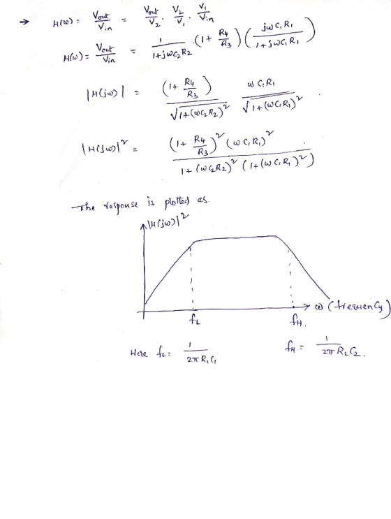
Homework Answers
Solution:
1) The first stage is a high pass filter circuit because at low frequency capacitor is open and does not allow the input and at high frequency capacitor is shorted and output is equal to input. It passes high frequency signals and attenuates low frequency signals.
Second stage is a DC amplifier with gain is equal to (1+R4/R3)
The third stage is a low pass filter circuit because at high frequency capacitor is open and allow the input and at low frequency capacitor is shorted and output is equal to zero. It passes low frequency signals and attenuates high frequency signals.
2) The total response is band pass response that will allow only signal frequencies between higher cutoff frequency fH and lower cutoff frequency fL.
3) Transfer function of each stage is found as,
Let output of first stage is taken as V1.
By voltage divider rule,
Capacitive reactance = Xc = 1/jwC1


Second stage, the transfer function is given by,
Let V2 be output voltage of second stage, and assume that op-amp is assumed to be ideal,

Transfer function of third stage is found as,
By voltage divider rule,
Capacitive reactance = Xc = 1/jwC2


4) The magnitude of the transfer function is given by,
Add Answer to:
Problem #1 (100pts) Consider the circuit shown in the Figure of three simpler circuits (stages). 1) Without solving...
Problem 4: For the following RLC circuit, R-1.01 kQ, 100 mH and C-0.1 μF. 1. Find...
 Problem 4: For the following RLC circuit, R-1.01 kQ, 100 mH and C-0.1 μF. 1. Find the transfer function H(jo) = Vo(jo)Vi(jo) 2. Find the gain of the transfer function | H(o) 3. Determin 4. Find the phase Ф(c) of the transfer function 5. Find Vo(t) if Vi(t) 100 cos(102 t) +60 cos (101 t) + 10 cos(106t) e the type of the filter. b) c) RVout Lo VoutVin Vin Vin Vin Vout Vout
QUESTION #2 PLEASE 1. Derive the transfer function for the circuit shown below. Plot H(s) versus...
 QUESTION #2 PLEASE
1. Derive the transfer function for the circuit shown below. Plot H(s) versus frequency in Hertz, on a semilog scale. Ri 11.3 k Ri 22.6 k R R = 68.1 kN R3 C C 0.01 uF R2 Vout(s) Vin(s) C2 10 (s+5) H(s) = (s+100)(s5000) , (a) draw the magnitude Bode plot 2. For the transfer function and find the approximate maximum value of (H(jw) in dB, (b) find the value of w where 1 for w>5...
QUESTION #2 PLEASE
1. Derive the transfer function for the circuit shown below. Plot H(s) versus frequency in Hertz, on a semilog scale. Ri 11.3 k Ri 22.6 k R R = 68.1 kN R3 C C 0.01 uF R2 Vout(s) Vin(s) C2 10 (s+5) H(s) = (s+100)(s5000) , (a) draw the magnitude Bode plot 2. For the transfer function and find the approximate maximum value of (H(jw) in dB, (b) find the value of w where 1 for w>5...
Problem 1: /25 For the circuit shown below, use frequency-domain circuit analysis techniques to determine (a)...
 Problem 1: /25 For the circuit shown below, use frequency-domain circuit analysis techniques to determine (a) the voltage transfer function Ho) of the circuit; (b) the magnitude response H(o) of the circuit; and (c) the phase response (0) of the circuit. (d) Based on the results of parts (a) - (c), identify the type of filter circuit shown. R + Vin(t) llll L Vout(t)
1. Find the transfer function Voda)/Vin(a) for the circuit shown in Figure 1 of the lab (where co...
 Please answer number 1
1. Find the transfer function Voda)/Vin(a) for the circuit shown in Figure 1 of the lab (where complex frequency variable s jo can be substituted for ease of analysis.) Calculate values for R and C such that the phase shift between the output and input is zero for an input frequency of 10kHz. What is the amplitude ratio (gain) of the output to the input at this frequency. 2. The RC network in figure 3 of...
Please answer number 1
1. Find the transfer function Voda)/Vin(a) for the circuit shown in Figure 1 of the lab (where complex frequency variable s jo can be substituted for ease of analysis.) Calculate values for R and C such that the phase shift between the output and input is zero for an input frequency of 10kHz. What is the amplitude ratio (gain) of the output to the input at this frequency. 2. The RC network in figure 3 of...
who can solve this problem? thanks Problem 3: Chain rule and circuit design Consider the circuit in the below figure...
 who can solve this problem? thanks
Problem 3: Chain rule and circuit design Consider the circuit in the below figure. You can as me zero initial conditions. t WW-어 2R L stage 1 stage 3 stage 4 stage 2 Part I: Redraw the above circuit in the s-domain and compute the transfer functions Ti(s), T(s). Tfs), Tds) of each one stages Part II: Somebody with a rusty recollection of linear circuits analyzed the above circuit and concluded that the transfer...
who can solve this problem? thanks
Problem 3: Chain rule and circuit design Consider the circuit in the below figure. You can as me zero initial conditions. t WW-어 2R L stage 1 stage 3 stage 4 stage 2 Part I: Redraw the above circuit in the s-domain and compute the transfer functions Ti(s), T(s). Tfs), Tds) of each one stages Part II: Somebody with a rusty recollection of linear circuits analyzed the above circuit and concluded that the transfer...
Consider the circuit shown in the figure(Figure 1). Suppose the four resistors in this circuit have...
 Consider the circuit shown in the figure(Figure 1). Suppose the four resistors in this circuit have the values R1 = 12 12, R2 = 7.0 N, R3 = 7.9 2 , and R4 = 12 12, and that the emf of the battery is € = 18 V You may want to review (Pages 748 - 751) Part A Find the current through each resistor using the rules for series and parallel resistors. Express vour answers using two significant figures...
PROBLEM #1: The circuit shown in Figure P4.4 consists of the cascade connection of three sections....
 PROBLEM #1: The circuit shown in Figure P4.4 consists of the cascade connection of three sections. In the total circuit all C's are equal and all R's are equal. (a) Let V= 0 and find the transfer function T(s) = (8) (b) Connect node 0 to node 2 such that V. =V,, and determine the transfer function under this condition. V (S) linn -- R +013 + RS FIGURE P4.4
Prelab Preparation: For the RC circuit shown in Figure 1, derive the modeling equation relating the output volta ge...
 Prelab Preparation: For the RC circuit shown in Figure 1, derive the modeling equation relating the output volta ge Vout to the input voltage vin. What is the transfer function? What is the time constant of the system? Vout Figure 1: RC Circuit What is the analytical step response solution in terms of vin, Rand C? For assumed values of R 1 K, and C 6.8 uF, perform a simulation using Matlab/Simulink assuming an input square wave signal of 5Vpp,...
Prelab 10.1: Active lowpass filter Given the circuit shown in Figure 10.1 with Ri-R2-Rs-R4-R-1.0 [k2, and...
 Prelab 10.1: Active lowpass filter Given the circuit shown in Figure 10.1 with Ri-R2-Rs-R4-R-1.0 [k2, and C 0.1 [uF (a) Represent the circuit in state-space form given by i(t) = ar(t) + bu(t), i.e., find the values of parameters a, b, c, and d. (b) Find the expression for the transfer function, G(s) the complex frequency (Laplace) domain. (c) Find the expression of the frequency transfer function H(f) and the value of the half power frequency, fB in Hz (d)...
5. [RC Circuits] Consider the circuit shown in Figure 5 attached. As shown, the switch is...
 5. [RC Circuits] Consider the circuit shown in Figure 5 attached. As shown, the switch is in position "A" for t < 0, and the circuit has been at rest for a long time. At time t = 0, the switch opens and the capacitor starts to drain across the resistor. (a) When the switch is closed and there is only a direct current (DC) source, the capacitor acts like an open circuit. Find the constant voltage across the capacitor...
 Problem 4: For the following RLC circuit, R-1.01 kQ, 100 mH and C-0.1 μF. 1. Find the transfer function H(jo) = Vo(jo)Vi(jo) 2. Find the gain of the transfer function | H(o) 3. Determin 4. Find the phase Ф(c) of the transfer function 5. Find Vo(t) if Vi(t) 100 cos(102 t) +60 cos (101 t) + 10 cos(106t) e the type of the filter. b) c) RVout Lo VoutVin Vin Vin Vin Vout Vout
 QUESTION #2 PLEASE
1. Derive the transfer function for the circuit shown below. Plot H(s) versus frequency in Hertz, on a semilog scale. Ri 11.3 k Ri 22.6 k R R = 68.1 kN R3 C C 0.01 uF R2 Vout(s) Vin(s) C2 10 (s+5) H(s) = (s+100)(s5000) , (a) draw the magnitude Bode plot 2. For the transfer function and find the approximate maximum value of (H(jw) in dB, (b) find the value of w where 1 for w>5...
QUESTION #2 PLEASE
1. Derive the transfer function for the circuit shown below. Plot H(s) versus frequency in Hertz, on a semilog scale. Ri 11.3 k Ri 22.6 k R R = 68.1 kN R3 C C 0.01 uF R2 Vout(s) Vin(s) C2 10 (s+5) H(s) = (s+100)(s5000) , (a) draw the magnitude Bode plot 2. For the transfer function and find the approximate maximum value of (H(jw) in dB, (b) find the value of w where 1 for w>5...
 Problem 1: /25 For the circuit shown below, use frequency-domain circuit analysis techniques to determine (a) the voltage transfer function Ho) of the circuit; (b) the magnitude response H(o) of the circuit; and (c) the phase response (0) of the circuit. (d) Based on the results of parts (a) - (c), identify the type of filter circuit shown. R + Vin(t) llll L Vout(t)
 Please answer number 1
1. Find the transfer function Voda)/Vin(a) for the circuit shown in Figure 1 of the lab (where complex frequency variable s jo can be substituted for ease of analysis.) Calculate values for R and C such that the phase shift between the output and input is zero for an input frequency of 10kHz. What is the amplitude ratio (gain) of the output to the input at this frequency. 2. The RC network in figure 3 of...
Please answer number 1
1. Find the transfer function Voda)/Vin(a) for the circuit shown in Figure 1 of the lab (where complex frequency variable s jo can be substituted for ease of analysis.) Calculate values for R and C such that the phase shift between the output and input is zero for an input frequency of 10kHz. What is the amplitude ratio (gain) of the output to the input at this frequency. 2. The RC network in figure 3 of...
 who can solve this problem? thanks
Problem 3: Chain rule and circuit design Consider the circuit in the below figure. You can as me zero initial conditions. t WW-어 2R L stage 1 stage 3 stage 4 stage 2 Part I: Redraw the above circuit in the s-domain and compute the transfer functions Ti(s), T(s). Tfs), Tds) of each one stages Part II: Somebody with a rusty recollection of linear circuits analyzed the above circuit and concluded that the transfer...
who can solve this problem? thanks
Problem 3: Chain rule and circuit design Consider the circuit in the below figure. You can as me zero initial conditions. t WW-어 2R L stage 1 stage 3 stage 4 stage 2 Part I: Redraw the above circuit in the s-domain and compute the transfer functions Ti(s), T(s). Tfs), Tds) of each one stages Part II: Somebody with a rusty recollection of linear circuits analyzed the above circuit and concluded that the transfer...
 Consider the circuit shown in the figure(Figure 1). Suppose the four resistors in this circuit have the values R1 = 12 12, R2 = 7.0 N, R3 = 7.9 2 , and R4 = 12 12, and that the emf of the battery is € = 18 V You may want to review (Pages 748 - 751) Part A Find the current through each resistor using the rules for series and parallel resistors. Express vour answers using two significant figures...
 PROBLEM #1: The circuit shown in Figure P4.4 consists of the cascade connection of three sections. In the total circuit all C's are equal and all R's are equal. (a) Let V= 0 and find the transfer function T(s) = (8) (b) Connect node 0 to node 2 such that V. =V,, and determine the transfer function under this condition. V (S) linn -- R +013 + RS FIGURE P4.4
 Prelab Preparation: For the RC circuit shown in Figure 1, derive the modeling equation relating the output volta ge Vout to the input voltage vin. What is the transfer function? What is the time constant of the system? Vout Figure 1: RC Circuit What is the analytical step response solution in terms of vin, Rand C? For assumed values of R 1 K, and C 6.8 uF, perform a simulation using Matlab/Simulink assuming an input square wave signal of 5Vpp,...
 Prelab 10.1: Active lowpass filter Given the circuit shown in Figure 10.1 with Ri-R2-Rs-R4-R-1.0 [k2, and C 0.1 [uF (a) Represent the circuit in state-space form given by i(t) = ar(t) + bu(t), i.e., find the values of parameters a, b, c, and d. (b) Find the expression for the transfer function, G(s) the complex frequency (Laplace) domain. (c) Find the expression of the frequency transfer function H(f) and the value of the half power frequency, fB in Hz (d)...
 5. [RC Circuits] Consider the circuit shown in Figure 5 attached. As shown, the switch is in position "A" for t < 0, and the circuit has been at rest for a long time. At time t = 0, the switch opens and the capacitor starts to drain across the resistor. (a) When the switch is closed and there is only a direct current (DC) source, the capacitor acts like an open circuit. Find the constant voltage across the capacitor...
Most questions answered within 3 hours.
-
Where is the error in this code sequence?
String s1 = "Hello";
String s2 = "ello";...
asked 10 months ago -
Financial data for Joel de Paris, Inc., for last year
follow:
Joel de Paris, Inc.
Balance...
asked 10 months ago -
Consider this reaction:
Al2(SO4)3 (aq)+ BaCl3
(aq) Al2Cl6 (aq)- +
3BaSO4(s) . What is the...
asked 10 months ago -
Suppose that Savneet is considering increasing her
recent random sample from 20 car rentals to 40...
asked 10 months ago -
Trucks arrive at an unloading terminal at an average rate of 120
per hour.
Trucks arrive...
asked 10 months ago -
Why are methanol and ethanol completely soluble in water while
octanol is not very little soluble....
asked 10 months ago -
A facilities manager at a university reads in a research report
that the mean amount of...
asked 10 months ago -
When the CuSO4 is rehydrated by adding water to the anhydrous
compound, is this an endothermic...
asked 10 months ago -
A ray of sunlight is passing from diamond into crown glass; the
angle of incidence is...
asked 10 months ago -
A block of mass 0.249 kg is placed on top of a light, vertical
spring of...
asked 10 months ago -
how do the kidneys compensate in the presences of acidosis
a) trigger hyperventilate
b) reserve acid...
asked 10 months ago -
Question 501 pts
The rental rate of capital to the firm increases. Which of the
following...
asked 10 months ago