
Homework Answers

Add Answer to:
Q3 A MOSFET is used as a low-side switch to control a 15 2 resistive load...
Please answer all the parts of the question clearly and fully! Thank you! Numerical Answers: (b)...
 Please answer all the parts of the question clearly and fully!
Thank you!
Numerical Answers:
(b) (0.0 A, 24 V), (approximately 1.6 A, 0.32 V)
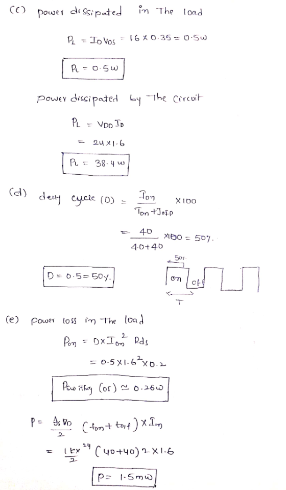
(c) 38.4 W, 0.5 W
(e) 0.26 W + 1.5 mW
SECTION B: Attempt any Two) questions 150 marks total! Q3 A MOSFET is used as a low-side switch to control a 15 2 resistive load from a 24 supply. The MOSFET has RDSan VDC 0.2 ? and ton-tof-40 ns. (a) Draw a suitable circuit....
Please answer all the parts of the question clearly and fully!
Thank you!
Numerical Answers:
(b) (0.0 A, 24 V), (approximately 1.6 A, 0.32 V)
(c) 38.4 W, 0.5 W
(e) 0.26 W + 1.5 mW
SECTION B: Attempt any Two) questions 150 marks total! Q3 A MOSFET is used as a low-side switch to control a 15 2 resistive load from a 24 supply. The MOSFET has RDSan VDC 0.2 ? and ton-tof-40 ns. (a) Draw a suitable circuit....
A MOSFET and diode is used in a circuit shown in figure. The operating conditions are...
A MOSFET and diode is used in a circuit shown in figure. The operating conditions are as follows: Input Voltage = VIN = 42 V, Io = 5A. Switching frequency fs = 400 kHz, Duty-cycle = D = 0.3. Diode Forward Voltage drop = 0.7V. Diode Peak Reverse Recovery Current = IRRM = 2.5 A. ON-state resistance of the MOSFET is RDS (on) = 25 mΩ. VGG as a step voltage between 0V and 10 V. MOSFET timings – Td...
1. A step-down chopper is connected to a 90VDC source and a 3Ω resistive load. The...
1. A step-down chopper is connected to a 90VDC source and a 3Ω resistive load. The chopper switching frequency is 5kHz with a 40% duty-cycle (D) Average free-wheeling diode current 2. A step-down chopper is connected to a 90VDC source and a 3Ω resistive load. The chopper switching frequency is 5kHz with a 40% duty-cycle (D) Size of inductance for a 10% peak-to-peak current ripple 3. VS = 90V EMF = 40V R = 2Ω L = 10mH switching frequency = 5kHz...
To design a high efficiency d.c., to d.c power converter with the given specifications min 10V max 15V nominal (regulated) 8V Input voltage: Output voltage: Nominal load current: 4A Inductor current...
 To design a high efficiency d.c., to d.c power converter with the given specifications min 10V max 15V nominal (regulated) 8V Input voltage: Output voltage: Nominal load current: 4A Inductor current ripple: 0.1A max Switching frequency: 30 kHz Output voltage ripple: 20 mV Define a suitable power circuit topology to meet the above specification? Sketch a circuit diagram of the chosen power circuit topology (a) Define the minimum and maximum duty cycles assuming that the control circuit keeps the output...
Given: A MOSFET is used in a switching power-pole found in Fig. 2-4a of the text....
 Given: A MOSFET is used in a switching power-pole found in Fig. 2-4a of the text. The operating conditions are as follows: Vin 35V, 6 A, the switching frequency fs 300 kHz, and the duty ratio d 0.4 a) Consider the diode in the power pole. Assuming an offset voltage forward bias model of the free-wheeling diode in which VM 1.2 V, calculate the average forward power loss in the diode HINT: Consider Eq. 2A-1 b) In the diode reverse...
a9a resistive load. Inductor 3-(35 pts) Design a converter that has an input voltage of 24 V DC and supplies 18 V DC to current is desired to be continuous and must not change more than 30 % of i...
 a9a resistive load. Inductor 3-(35 pts) Design a converter that has an input voltage of 24 V DC and supplies 18 V DC to current is desired to be continuous and must not change more than 30 % of its average value voltage ripple must be lower than 2 %. Switching frequency is 10 kHz. a) Draw the circuit diagram. Calculate the duty ratio. Calculate values for 2 desired conditions of the inductor current and determine the value of the...
1. to design a high efficiency d.c. to d.c. power converter with the given specifications Input v...
 1. to design a high efficiency d.c. to d.c. power converter with the given specifications Input voltage Output voltage Nominal load current: 4A Inductor current ripple: 0.1A max Switching frequency: 30 kHz Output voltage ripple: 20 mV min 10V max 15V nominal (regulated) 8V Define a suitable power circuit topology to meet the above specification Sketch a circuit diagram of the chosen power circuit topology (a) Define the minimum and maximum duty cycles assuming that the control circuit keeps the...
Problem 2: Pulse width modulation (PWM) is a method of reducing the average power delivered by...
 Problem 2: Pulse width modulation (PWM) is a method of reducing the average power delivered by an electrical signal, by effectively chopping it up into discrete parts. The average value of voltage fed to the load is controlled by turning the switch between supply and load on and off at a fast rate. The longer the switch is on compared to the off periods, the higher the total power supplied to the load. PWM is particularly suited for running DC...
Design a boost converter power stage to the following specification: Input voltage Output voltage: Output voltage...
 Design a boost converter power stage to the following specification: Input voltage Output voltage: Output voltage ripple:max 20mV Load power: Switching frequency: 15kHz 110-125V 300V 1.5kW Calculate: (i) Maximum duty cycle (ii) Minimum duty cycle (iii) Average diode current (iv) Assuming the Rds(on) of the MOSFET is 0.01 Ω, and the diode forward voltage is 0.8V, calculate the approximate efficiency of the circuit. 2. A switching power supply shown in the circuit below has its switch driven by a signal...
Design a common-source MOSFET amplifier such that RG is a multiple of D = o.st mot...
 Design a common-source MOSFET amplifier such that RG is a multiple of D = o.st mot (Avol 15.02 VN RL = 17kr • Choose a sinusoidal signal voltage, Vsig, with Rsig = 400 kN to use as the input in this problem. Use 2 kHz as the frequency of your sinusoidal. This is a design problem so vsig will not be unique. Use V+ = 0.8 V, k = 5 mA/V2, and VA = 80 V for your MOSFET. Assume...
 Please answer all the parts of the question clearly and fully!
Thank you!
Numerical Answers:
(b) (0.0 A, 24 V), (approximately 1.6 A, 0.32 V)
(c) 38.4 W, 0.5 W
(e) 0.26 W + 1.5 mW
SECTION B: Attempt any Two) questions 150 marks total! Q3 A MOSFET is used as a low-side switch to control a 15 2 resistive load from a 24 supply. The MOSFET has RDSan VDC 0.2 ? and ton-tof-40 ns. (a) Draw a suitable circuit....
Please answer all the parts of the question clearly and fully!
Thank you!
Numerical Answers:
(b) (0.0 A, 24 V), (approximately 1.6 A, 0.32 V)
(c) 38.4 W, 0.5 W
(e) 0.26 W + 1.5 mW
SECTION B: Attempt any Two) questions 150 marks total! Q3 A MOSFET is used as a low-side switch to control a 15 2 resistive load from a 24 supply. The MOSFET has RDSan VDC 0.2 ? and ton-tof-40 ns. (a) Draw a suitable circuit....
 To design a high efficiency d.c., to d.c power converter with the given specifications min 10V max 15V nominal (regulated) 8V Input voltage: Output voltage: Nominal load current: 4A Inductor current ripple: 0.1A max Switching frequency: 30 kHz Output voltage ripple: 20 mV Define a suitable power circuit topology to meet the above specification? Sketch a circuit diagram of the chosen power circuit topology (a) Define the minimum and maximum duty cycles assuming that the control circuit keeps the output...
 Given: A MOSFET is used in a switching power-pole found in Fig. 2-4a of the text. The operating conditions are as follows: Vin 35V, 6 A, the switching frequency fs 300 kHz, and the duty ratio d 0.4 a) Consider the diode in the power pole. Assuming an offset voltage forward bias model of the free-wheeling diode in which VM 1.2 V, calculate the average forward power loss in the diode HINT: Consider Eq. 2A-1 b) In the diode reverse...
 a9a resistive load. Inductor 3-(35 pts) Design a converter that has an input voltage of 24 V DC and supplies 18 V DC to current is desired to be continuous and must not change more than 30 % of its average value voltage ripple must be lower than 2 %. Switching frequency is 10 kHz. a) Draw the circuit diagram. Calculate the duty ratio. Calculate values for 2 desired conditions of the inductor current and determine the value of the...
 1. to design a high efficiency d.c. to d.c. power converter with the given specifications Input voltage Output voltage Nominal load current: 4A Inductor current ripple: 0.1A max Switching frequency: 30 kHz Output voltage ripple: 20 mV min 10V max 15V nominal (regulated) 8V Define a suitable power circuit topology to meet the above specification Sketch a circuit diagram of the chosen power circuit topology (a) Define the minimum and maximum duty cycles assuming that the control circuit keeps the...
 Problem 2: Pulse width modulation (PWM) is a method of reducing the average power delivered by an electrical signal, by effectively chopping it up into discrete parts. The average value of voltage fed to the load is controlled by turning the switch between supply and load on and off at a fast rate. The longer the switch is on compared to the off periods, the higher the total power supplied to the load. PWM is particularly suited for running DC...
 Design a boost converter power stage to the following specification: Input voltage Output voltage: Output voltage ripple:max 20mV Load power: Switching frequency: 15kHz 110-125V 300V 1.5kW Calculate: (i) Maximum duty cycle (ii) Minimum duty cycle (iii) Average diode current (iv) Assuming the Rds(on) of the MOSFET is 0.01 Ω, and the diode forward voltage is 0.8V, calculate the approximate efficiency of the circuit. 2. A switching power supply shown in the circuit below has its switch driven by a signal...
 Design a common-source MOSFET amplifier such that RG is a multiple of D = o.st mot (Avol 15.02 VN RL = 17kr • Choose a sinusoidal signal voltage, Vsig, with Rsig = 400 kN to use as the input in this problem. Use 2 kHz as the frequency of your sinusoidal. This is a design problem so vsig will not be unique. Use V+ = 0.8 V, k = 5 mA/V2, and VA = 80 V for your MOSFET. Assume...
Most questions answered within 3 hours.
-
Where is the error in this code sequence?
String s1 = "Hello";
String s2 = "ello";...
asked 11 months ago -
Financial data for Joel de Paris, Inc., for last year
follow:
Joel de Paris, Inc.
Balance...
asked 11 months ago -
Consider this reaction:
Al2(SO4)3 (aq)+ BaCl3
(aq) Al2Cl6 (aq)- +
3BaSO4(s) . What is the...
asked 11 months ago -
Suppose that Savneet is considering increasing her
recent random sample from 20 car rentals to 40...
asked 11 months ago -
Trucks arrive at an unloading terminal at an average rate of 120
per hour.
Trucks arrive...
asked 11 months ago -
Why are methanol and ethanol completely soluble in water while
octanol is not very little soluble....
asked 11 months ago -
A facilities manager at a university reads in a research report
that the mean amount of...
asked 11 months ago -
When the CuSO4 is rehydrated by adding water to the anhydrous
compound, is this an endothermic...
asked 11 months ago -
A ray of sunlight is passing from diamond into crown glass; the
angle of incidence is...
asked 11 months ago -
A block of mass 0.249 kg is placed on top of a light, vertical
spring of...
asked 11 months ago -
how do the kidneys compensate in the presences of acidosis
a) trigger hyperventilate
b) reserve acid...
asked 11 months ago -
Question 501 pts
The rental rate of capital to the firm increases. Which of the
following...
asked 11 months ago