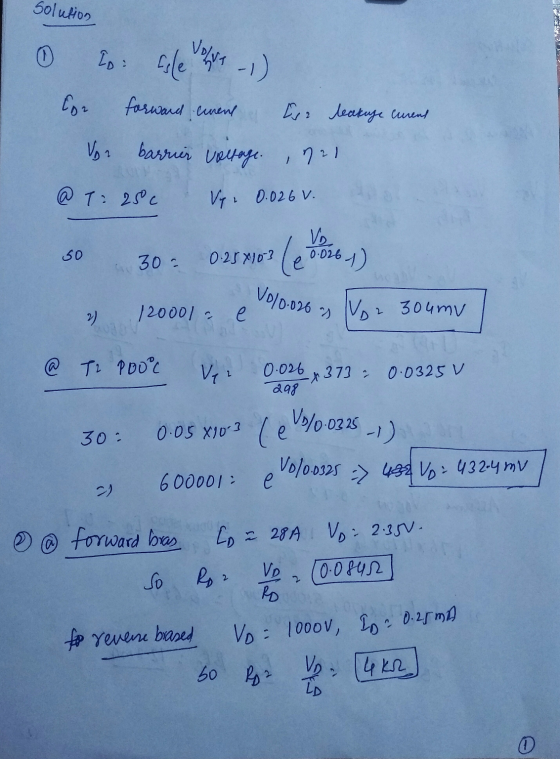
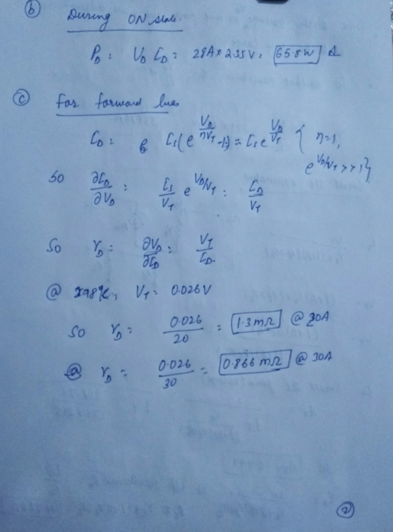
![Tutorial 2 The data sheet of a certain P-N junction diode specifies a leakage current of 0.25mA at room temperature of 25[]C](http://img.homeworklib.com/questions/71305af0-053b-11eb-a3b7-0d8e0198b74b.png?x-oss-process=image/resize,w_560)
Homework Answers
Add Answer to:
Tutorial 2 The data sheet of a certain P-N junction diode specifies a leakage current of...
DIODE CHARACTERISTICS Objective: The objective of this laboratory is to examine and plot the forward characteristics...
 DIODE CHARACTERISTICS Objective: The objective of this laboratory is to examine and plot the forward characteristics curve of a p-n junction diode and become familiar with the characteristics of both the p-n junction diode and the light emitting diode (LED). Prelab: Answer the following on a separate sheet of paper. Show your work and box your answers 1. Review the data sheets for the IN4001 p-n junction diode and answer the following a) Determine the maximum forward current and the...
The doping and geometric parameters of a P–N junction diode are: - ND = 10^20 cm−3,...
The doping and geometric parameters of a P–N junction diode are: - ND = 10^20 cm−3, Wcathode = 1 μm <<Lp, - NA = 5 × 10^15 cm−3, Wanode = 10 μm <<Ln, - Junction area AJ = 500 × 500 μm2. Calculate the reverse biasing current IS, and then use this result to obtain the forward voltage that corresponds to a current of 100 mA, if the semiconductor material is: (a) Si (μn = 1450 cm2/V · s, μp...
1. a) State the diode equation and explain the significance of each term. b) Sketch the current - voltage characteristics for a typical silicon diode over the 4 voltage range -2 V to +2 V. Explai...
 1. a) State the diode equation and explain the significance of each term. b) Sketch the current - voltage characteristics for a typical silicon diode over the 4 voltage range -2 V to +2 V. Explain how the characteristics would change if the diode was fabricated using germanium. Give an equivalent circuit representation of the device in each case. c) In a silicon diode a current of 200 HA flows when a forward bias voltage of 0.5 V4 is applied...
Ctri Question 3 (20 Marks) Lab 1-Zener Circuits and Applications Theory: Zener diode is designed ...
 Ctri Question 3 (20 Marks) Lab 1-Zener Circuits and Applications Theory: Zener diode is designed to operate in reverse conduction. Zener breakdown occurs at a precisely defined voltage, allowing the diode to be used as a voltage reference or clipper. While Zener diodes are usually operated in reverse conduction, they may also be operated in cutoff and forward conduction. There are two different effects that are used in "Zener diodes". The only practical difference is that the two types have...
2. True or false: a. Schottky barrier diodes typically have lower leakage current than p-n junction...
 2. True or false: a. Schottky barrier diodes typically have lower leakage current than p-n junction diodes b. The semiconductor drift current is proportional to the magnitude of the electric field. c. The ideal subthreshold slope for a MOSFET increases with increasing temperature d. For a MOSFET the density of inversion-layer charge is QinrsonCx VGS VFB e. For a MOSFET the following equation is correct: on inversion -Raccumulation VGS-VFB f. For a BJT the following equation is correct: -- 1-a...
2. An abrupt silicon p-n junction is formed from p-type material with a resistivity of 1.3x10-...
 2. An abrupt silicon p-n junction is formed from p-type material with a resistivity of 1.3x10- 12m and n-type material with resistivity of 4.6x10- Sam at room temperature. The lifetimes of the p- and n-materials are 100 us and 150 us respectively, and the junction area is 1.0 mm?.if Mp 4.8x10² m²/V.s „Mn = 0.135 m²/V.s and n; = 1.5x10¹⁶ carrier /m , calculate the reverse bias leakage current. Then calculate forward bias current if a 0.3 volt is applied.
For the double diode circuit shown in figure 2-1, answer the following questions. In Figure 2-1...
 For the double diode circuit shown in figure 2-1, answer the following questions. In Figure 2-1 a) (10pts) For the triangular wave input shown (Vin), sketch the output voltage (Vout) using the constant voltage drop model (CVD: Vo-0.7V). Be sure to note the voltage values on the y-axis of your Vout plot and show any equations you used to determine those values ime FEE 334: Spring 2019 Midterm b) (2pts) During the middle of the first time segment (when Vin...
Design an abrupt Si p+-n junction diode that has a reverse breakdown voltage of 130 V and has a forward-bias current of 2.2 mA at V = 0.7 volt. Assume tp = l0^-7 s.
Design an abrupt Sip+-n junction diode that has a reverse breakdown voltage of 130 V andhas a forward-bias current of 2.2 mA at V = 0.7 volt. Assume tp = l0^-7 s.
A pn junction diode is made of a new semiconductor with 10^16cm-3 acceptors in the p...
A pn junction diode is made of a new semiconductor with 10^16cm-3 acceptors in the p side and 2x10^17cm-3 donors on the n-side. Intrinsic carrier concentration is same as silicon 10^10cm-3 at room temperature. Let's assume that a forward bias voltage is applied in a way that it create following minority carrier concentrations in quasi neutral regions. n(x) =10^4 - 10^14/[10^4(x+xp)-1] (cm-3) where x<xp<0 and p(x) = 500+10^15/[10^4(x+xn)+1] (cm-3) where x>xn>0. x is given in cm scale. Calculate the total...
A pn junction diode is made of a new semiconductor with 10^16cm-3 donors in the n...
A pn junction diode is made of a new semiconductor with 10^16cm-3 donors in the n side and 2x10^17cm-3 acceptors on the p-side. Intrinsic carrier concentration is same as silicon 10^10cm-3at room temperature. Let's assume that a forward bias voltage is applied in a way that it create following minority carrier concentrations in quasi neutral regions. p(x) =10^4 + 10^14/[1+10^4(x-xn)] (cm-3) where x>xn>0 and n(x) = 500-10^15/[10^4(x+xp)-1] (cm-3) where x<-xp<0. x is given in cm scale. Calculate the total current...
 DIODE CHARACTERISTICS Objective: The objective of this laboratory is to examine and plot the forward characteristics curve of a p-n junction diode and become familiar with the characteristics of both the p-n junction diode and the light emitting diode (LED). Prelab: Answer the following on a separate sheet of paper. Show your work and box your answers 1. Review the data sheets for the IN4001 p-n junction diode and answer the following a) Determine the maximum forward current and the...
 1. a) State the diode equation and explain the significance of each term. b) Sketch the current - voltage characteristics for a typical silicon diode over the 4 voltage range -2 V to +2 V. Explain how the characteristics would change if the diode was fabricated using germanium. Give an equivalent circuit representation of the device in each case. c) In a silicon diode a current of 200 HA flows when a forward bias voltage of 0.5 V4 is applied...
 Ctri Question 3 (20 Marks) Lab 1-Zener Circuits and Applications Theory: Zener diode is designed to operate in reverse conduction. Zener breakdown occurs at a precisely defined voltage, allowing the diode to be used as a voltage reference or clipper. While Zener diodes are usually operated in reverse conduction, they may also be operated in cutoff and forward conduction. There are two different effects that are used in "Zener diodes". The only practical difference is that the two types have...
 2. True or false: a. Schottky barrier diodes typically have lower leakage current than p-n junction diodes b. The semiconductor drift current is proportional to the magnitude of the electric field. c. The ideal subthreshold slope for a MOSFET increases with increasing temperature d. For a MOSFET the density of inversion-layer charge is QinrsonCx VGS VFB e. For a MOSFET the following equation is correct: on inversion -Raccumulation VGS-VFB f. For a BJT the following equation is correct: -- 1-a...
 2. An abrupt silicon p-n junction is formed from p-type material with a resistivity of 1.3x10- 12m and n-type material with resistivity of 4.6x10- Sam at room temperature. The lifetimes of the p- and n-materials are 100 us and 150 us respectively, and the junction area is 1.0 mm?.if Mp 4.8x10² m²/V.s „Mn = 0.135 m²/V.s and n; = 1.5x10¹⁶ carrier /m , calculate the reverse bias leakage current. Then calculate forward bias current if a 0.3 volt is applied.
 For the double diode circuit shown in figure 2-1, answer the following questions. In Figure 2-1 a) (10pts) For the triangular wave input shown (Vin), sketch the output voltage (Vout) using the constant voltage drop model (CVD: Vo-0.7V). Be sure to note the voltage values on the y-axis of your Vout plot and show any equations you used to determine those values ime FEE 334: Spring 2019 Midterm b) (2pts) During the middle of the first time segment (when Vin...
Most questions answered within 3 hours.
-
Where is the error in this code sequence?
String s1 = "Hello";
String s2 = "ello";...
asked 11 months ago -
Financial data for Joel de Paris, Inc., for last year
follow:
Joel de Paris, Inc.
Balance...
asked 11 months ago -
Consider this reaction:
Al2(SO4)3 (aq)+ BaCl3
(aq) Al2Cl6 (aq)- +
3BaSO4(s) . What is the...
asked 11 months ago -
Suppose that Savneet is considering increasing her
recent random sample from 20 car rentals to 40...
asked 11 months ago -
Trucks arrive at an unloading terminal at an average rate of 120
per hour.
Trucks arrive...
asked 11 months ago -
Why are methanol and ethanol completely soluble in water while
octanol is not very little soluble....
asked 11 months ago -
A facilities manager at a university reads in a research report
that the mean amount of...
asked 11 months ago -
When the CuSO4 is rehydrated by adding water to the anhydrous
compound, is this an endothermic...
asked 11 months ago -
A ray of sunlight is passing from diamond into crown glass; the
angle of incidence is...
asked 11 months ago -
A block of mass 0.249 kg is placed on top of a light, vertical
spring of...
asked 11 months ago -
how do the kidneys compensate in the presences of acidosis
a) trigger hyperventilate
b) reserve acid...
asked 11 months ago -
Question 501 pts
The rental rate of capital to the firm increases. Which of the
following...
asked 11 months ago